

Analyzing the Impact of Gate Oxide Screening on Interface Trap Density in SiC Power MOSFETs Using a Novel Temperature-Triggered Method

 ,
,  ,
,  , ,
, ,
Abstract
1. Introduction
2. Mathematical Analysis of the Temperature-Triggered Threshold Voltage Shift (T3VS) Method
3. Experimental Methodologies
3.1. Device Information
3.2. Experimental Methodology to Determine
3.3. SWAP Methodology
4. Results and Discussion
4.1. Extraction of Commercial 1.2 kV 4H-SiC MOSFETs Using T3VS Technique
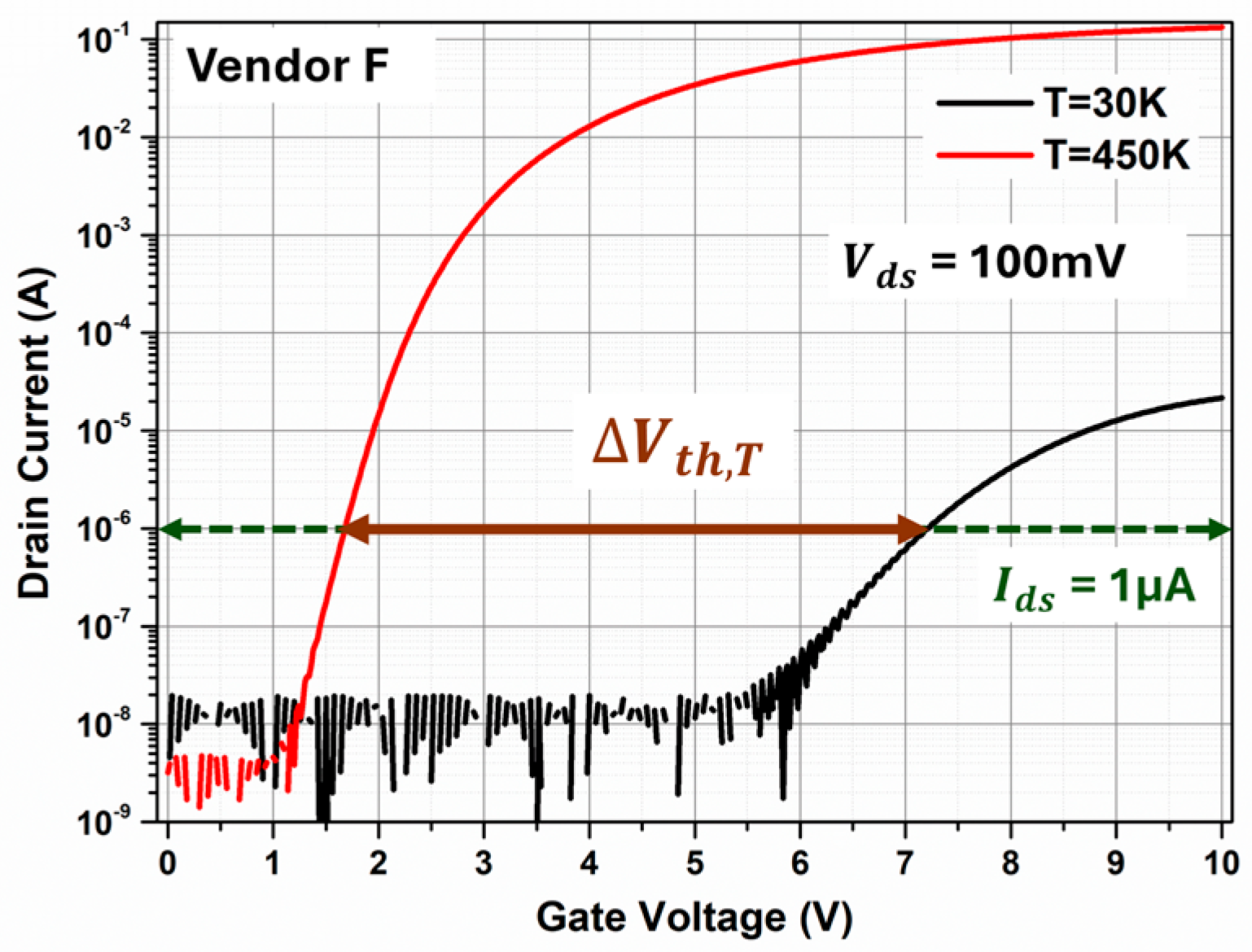
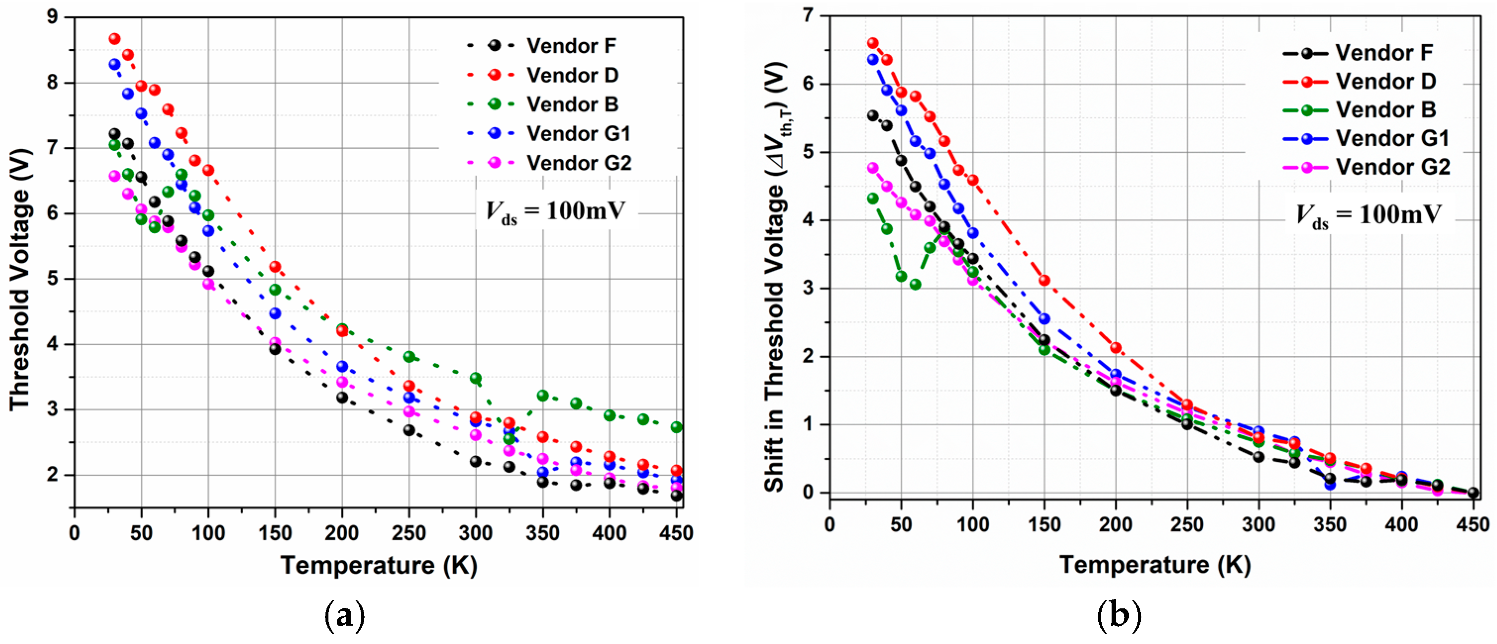
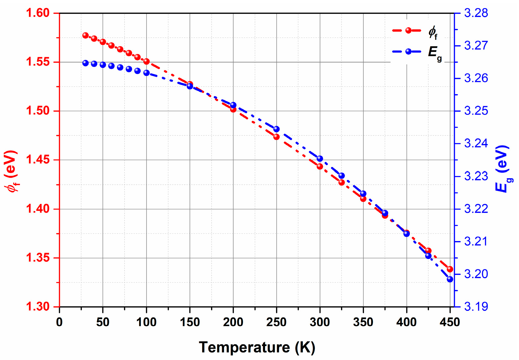
4.1.1. Effect of Temperature on of the DUTs
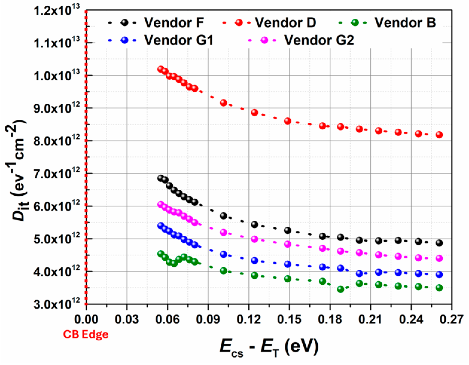
4.1.2. Baseline Profile Extraction
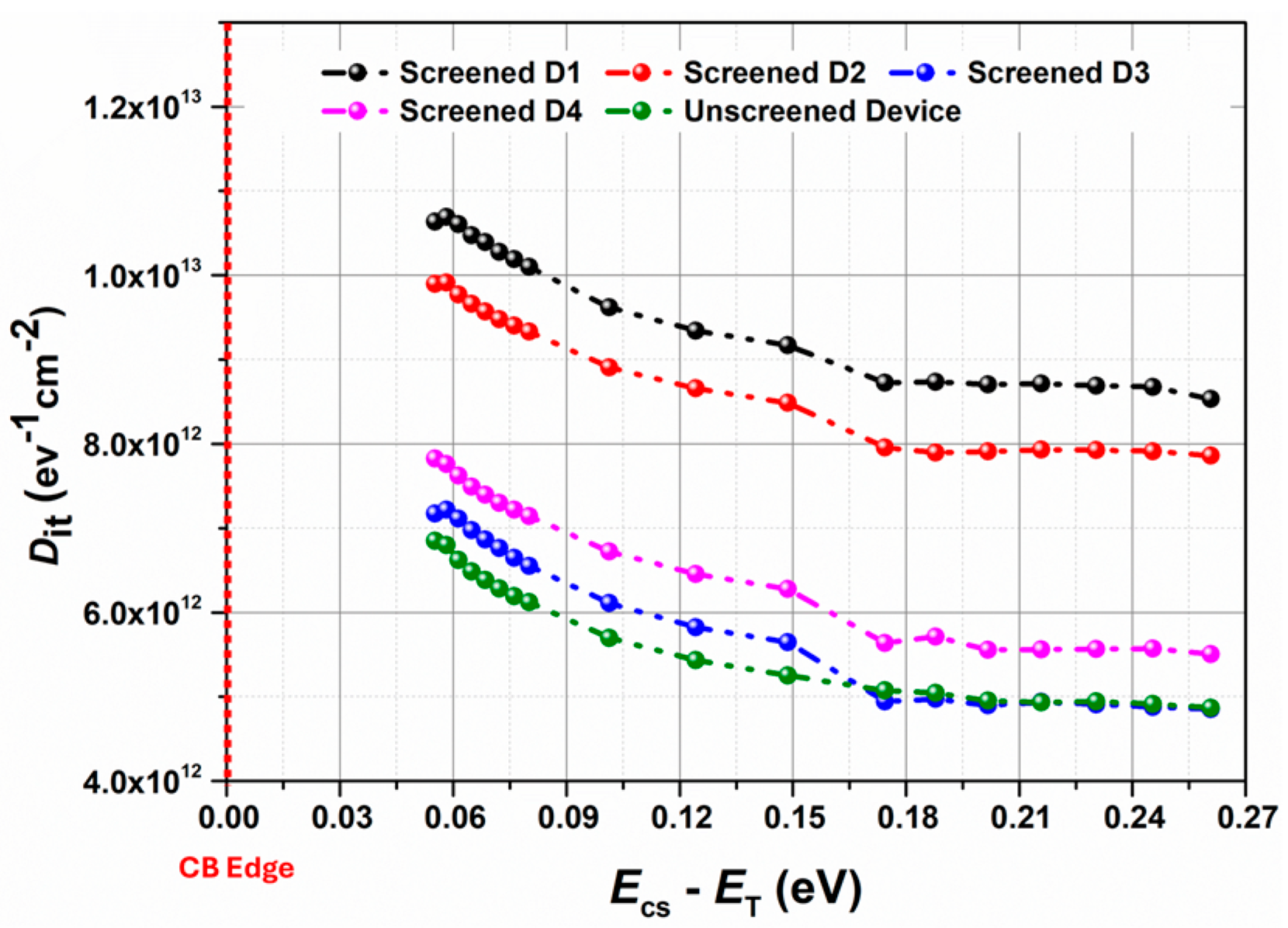
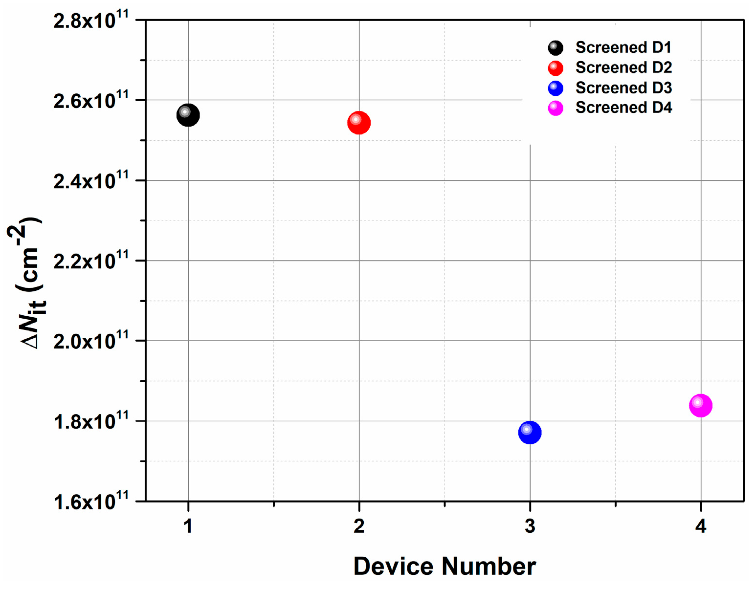
4.2. Effect of SWAP on Distribution
5. Conclusions
Author Contributions
Funding
Data Availability Statement
Conflicts of Interest
Abbreviations
| T3VS | temperature-triggered threshold voltage shift |
| SWAP | screening with adjustment pulse |
| MOSFET | metal oxide semiconductor field-effect transistor |
| DUT | device under test |
References
- Chaturvedi, M.; Dimitrijev, S.; Haasmann, D.; Moghadam, H.A.; Pande, P.; Jadli, U. Comparison of Commercial Planar and Trench SiC MOSFETs by Electrical Characterization of Performance-Degrading Near-Interface Traps. IEEE Trans. Electron Devices 2022, 69, 6225–6230. [Google Scholar] [CrossRef]
- Williams, R.K.; Darwish, M.N.; Blanchard, R.A.; Siemieniec, R.; Rutter, P.; Kawaguchi, Y. The Trench Power MOSFET: Part I—History, Technology, and Prospects. IEEE Trans. Electron Devices 2017, 64, 674–691. [Google Scholar] [CrossRef]
- Shi, L.; Qian, J.; Jin, M.; Bhattacharya, M.; Yu, H.; Shimbori, A.; White, M.H.; Agarwal, A.K. Investigation on gate oxide reliability under gate bias screening for commercial SiC planar and trench MOSFETs. Mater. Sci. Semicond. Process. 2024, 174, 108194. [Google Scholar] [CrossRef]
- Wu, L.; Liang, J.; Zhang, M.; Liu, M.; Zhang, T.; Yang, G.; Song, X. An approach for extracting the SiC/SiO2 SiC MOSFET interface trap distribution and study during short circuit. Mater. Sci. Semicond. Process. 2023, 163, 107581. [Google Scholar] [CrossRef]
- Zhong, X.; Jiang, H.; Qiu, G.; Tang, L.; Mao, H.; Chao, X.; Jiang, X.; Hu, J.; Qi, X.; Ran, L. Bias Temperature Instability of Silicon Carbide Power MOSFET under AC Gate Stresses. IEEE Trans. Power Electron. 2021, 37, 1998–2008. [Google Scholar] [CrossRef]
- Kimoto, T.; Watanabe, H. Defect engineering in SiC technology for high-voltage power devices. Appl. Phys. Express 2020, 13, 120101. [Google Scholar] [CrossRef]
- Berens, J.; Rasinger, F.; Aichinger, T.; Heuken, M.; Krieger, M.; Pobegen, G. Detection and Cryogenic Characterization of Defects at the SiO2/4H-SiC Interface in Trench MOSFET. IEEE Trans. Electron Devices 2019, 66, 1213–1217. [Google Scholar] [CrossRef]
- Lelis, A.J.; Green, R.; Habersat, D.B.; El, M. Basic Mechanisms of Threshold-Voltage Instability and Implications for Reliability Testing of SiC MOSFETs. IEEE Trans. Electron Devices 2015, 62, 316–323. [Google Scholar] [CrossRef]
- Yen, C.-T.; Hung, C.-C.; Hung, H.-T.; Lee, C.-Y.; Lee, L.-S.; Huang, Y.-F.; Hsu, F.-J. Negative bias temperature instability of SiC MOSFET induced by interface trap assisted hole trapping. Appl. Phys. Lett. 2016, 108, 012106. [Google Scholar] [CrossRef]
- Aichinger, T.; Rescher, G.; Pobegen, G. Threshold voltage peculiarities and bias temperature instabilities of SiC MOSFETs. Microelectron. Reliab. 2018, 80, 68–78. [Google Scholar] [CrossRef]
- Aichinger, T.; Schmidt, M. Gate-oxide reliability and failure-rate reduction of industrial SiC MOSFETs. In Proceedings of the 2020 IEEE International Reliability Physics Symposium (IRPS), Dallas, TX, USA, 28 April–30 May 2020; pp. 1–6. [Google Scholar]
- Lee, J.C.; Chen, I.-C.; Hu, C. Modeling and characterization of gate oxide reliability. IEEE Trans. Electron Devices 1988, 35, 2268–2278. [Google Scholar] [CrossRef]
- Ma, Z.J.; Lai, P.T.; Liu, Z.H.; Fleischer, S.; Cheng, Y.C. Tunneling-injection-induced turnaround behavior of threshold voltage in thermally nitrided oxide n-channel metal-oxide-semiconductor field-effect transistors. J. Appl. Phys. 1990, 68, 6299–6303. [Google Scholar] [CrossRef]
- DiMaria, D.; Cartier, E.; Buchanan, D. Anode hole injection and trapping in silicon dioxide. J. Appl. Phys. 1996, 80, 304–317. [Google Scholar] [CrossRef]
- Jin, M.; Bhattacharya, M.; Shi, L.; Qian, J.; Houshmand, S.; Yu, H.; White, M.H.; Agarwal, A.K.; Liu, T.; Zhu, S.; et al. Threshold Voltage Adjustment of Commercial SiC MOSFETs During Gate Oxide Screening by Low Field Pulse. In Proceedings of the 2024 IEEE 11th Workshop on Wide Bandgap Power Devices & Applications (WiPDA), Dayton, OH, USA, 4–6 November 2024; pp. 1–5. [Google Scholar]
- Wang, J.; Jiang, X. Review and analysis of SiC MOSFETs’ ruggedness and reliability. IET Power Electron. 2020, 13, 445–455. [Google Scholar] [CrossRef]
- Uranwala, J.S.; Simmons, J.G.; Mar, H.A. The determination of the energy distribution of interface traps in metal-nitride-oxide-silicon (memory) devices using non-steady-state techniques. Solid-State Electron. 1976, 19, 375–380. [Google Scholar] [CrossRef]
- Mar, H.A.; Simmons, J.G. A review of the techniques used to determine trap parameters in the MNOS structure. IEEE Trans. Electron Devices 1977, 24, 540–546. [Google Scholar] [CrossRef]
- Vidarsson, A.M.; Nicholls, J.R.; Haasmann, D.; Dimitrijev, S.; Sveinbjörnsson, E.Ö. Detection of near-interface traps in NO annealed 4H-SiC metal oxide semiconductor capacitors combining different electrical characterization methods. J. Appl. Phys. 2022, 131, 215702. [Google Scholar] [CrossRef]
- Yoshioka, H.; Nakamura, T.; Kimoto, T. Accurate evaluation of interface state density in SiC metal-oxide-semiconductor structures using surface potential based on depletion capacitance. J. Appl. Phys. 2012, 111, 014502. [Google Scholar] [CrossRef]
- Rudenko, T.E.; Ólafsson, H.Ö.; Sveinbjörnsson, E.Ö.; Osiyuk, I.P.; Tyagulski, I.P. Analysis of the electron traps at the 4H-SiC/SiO2 interface using combined CV/thermally stimulated current measurements. Microelectron. Eng. 2004, 72, 213–217. [Google Scholar] [CrossRef]
- Yonamoto, Y. Study on individual traps in metal–oxide–semiconductor field-effect transistors by means of thermally stimulated threshold voltage shift. J. Therm. Anal. Calorim. 2015, 122, 1299–1305. [Google Scholar] [CrossRef]
- Yu, S.; White, M.H.; Agarwal, A.K. Experimental determination of interface trap density and fixed positive oxide charge in commercial 4H-SiC power MOSFETs. IEEE Access 2021, 9, 149118–149124. [Google Scholar]
- Asllani, B.; Fayyaz, A.; Castellazzi, A.; Morel, H.; Planson, D. V subthreshold hysteresis technology and temperature dependence in commercial 4H-SiC MOSFETs. Microelectron. Reliab. 2018, 88–90, 604–609. [Google Scholar] [CrossRef]
- Asllani, B.; Castellazzi, A.; Salvado, O.A.; Fayyaz, A.; Morel, H.; Planson, D. VTH-Hysteresis and Interface States Characterisation in SiC Power MOSFETs with Planar and Trench Gate. In Proceedings of the 2019 IEEE International Reliability Physics Symposium (IRPS), Monterey, CA, USA, 31 March–4 April 2019; pp. 1–6. [Google Scholar]
- Penumatcha, A.V.; Swandono, S.; Cooper, J.A. Limitations of the High-Low C-V Technique for MOS Interfaces With Large Time Constant Dispersion. IEEE Trans. Electron Devices 2013, 60, 923–926. [Google Scholar] [CrossRef]
- Maddi, H.L.R.; Nayak, S.; Talesara, V.; Xu, Y.; Lu, W.; Agarwal, A.K. Characterization of Near Conduction Band SiC/SiO2 Interface Traps in Commercial 4H-SiC Power MOSFETs. In Proceedings of the 2022 IEEE 9th Workshop on Wide Bandgap Power Devices & Applications (WiPDA), Redondo Beach, CA, USA, 7–9 November 2022; pp. 22–25. [Google Scholar]
- Schwalke, U.; Pölzl, M.; Sekinger, T.; Kerber, M. Ultra-thick gate oxides: Charge generation and its impact on reliability. Microelectron. Reliab. 2001, 41, 1007–1010. [Google Scholar] [CrossRef]
- Matocha, K.; Dunne, G.; Soloviev, S.; Beaupre, R. Time-Dependent Dielectric Breakdown of 4H-SiC MOS Capacitors and DMOSFETs. IEEE Trans. Electron Devices 2008, 55, 1830–1834. [Google Scholar] [CrossRef]
- Kimoto, T.; Cooper, J.A. Fundamentals of Silicon Carbide Technology: Growth, Characterization, Devices and Applications; John Wiley & Sons: Hoboken, NJ, USA, 2014. [Google Scholar]
- Ziane, D.; Bluet, J.M.; Guillot, G.; Godignon, P.; Montserrat, J.; Ciechonski, R.; Syväjärvi, M.; Yakimova, R.; Chen, L.; Mawby, P.A. Characterizations of SiC/SiO2 interface quality toward high power MOSFETs realization. Mater. Sci. Forum 2004, 457–460, 1281–1286. [Google Scholar]
- Shi, L.; Qian, J.; Jin, M.; Bhattacharya, M.; Yu, H.; White, M.H.; Agarwal, A.K.; Shimbori, A. Evaluation of Burn-in Technique on Gate Oxide Reliability in Commercial SiC MOSFETs. In Proceedings of the 2024 IEEE International Reliability Physics Symposium (IRPS), Grapevine, TX, USA, 14–18 April 2024; pp. 1–6. [Google Scholar]


| Vendor | Structure | [nm] | Current Rating [A] | On-Resistance [mΩ] |
|---|---|---|---|---|
| F | Planar | 38 | 7.6 | 350 |
| D | Planar | 45 | 20 | 189 |
| B | Asymmetric trench | 57.1 | 4.7 | 350 |
| G1 | Double trench | 58.1 | 17 | 160 |
| G2 | Reinforced double trench | 39.6 | 26 | 62 |
Disclaimer/Publisher’s Note: The statements, opinions and data contained in all publications are solely those of the individual author(s) and contributor(s) and not of MDPI and/or the editor(s). MDPI and/or the editor(s) disclaim responsibility for any injury to people or property resulting from any ideas, methods, instructions or products referred to in the content. |
© 2025 by the authors. Licensee MDPI, Basel, Switzerland. This article is an open access article distributed under the terms and conditions of the Creative Commons Attribution (CC BY) license (https://creativecommons.org/licenses/by/4.0/).
Share and Cite
Bhattacharya, M.; Jin, M.; Yu, H.; Houshmand, S.; Qian, J.; White, M.H.; Shimbori, A.; Agarwal, A.K. Analyzing the Impact of Gate Oxide Screening on Interface Trap Density in SiC Power MOSFETs Using a Novel Temperature-Triggered Method. Micromachines 2025, 16, 371. https://doi.org/10.3390/mi16040371
Bhattacharya M, Jin M, Yu H, Houshmand S, Qian J, White MH, Shimbori A, Agarwal AK. Analyzing the Impact of Gate Oxide Screening on Interface Trap Density in SiC Power MOSFETs Using a Novel Temperature-Triggered Method. Micromachines. 2025; 16(4):371. https://doi.org/10.3390/mi16040371
Chicago/Turabian StyleBhattacharya, Monikuntala, Michael Jin, Hengyu Yu, Shiva Houshmand, Jiashu Qian, Marvin H. White, Atsushi Shimbori, and Anant K. Agarwal. 2025. "Analyzing the Impact of Gate Oxide Screening on Interface Trap Density in SiC Power MOSFETs Using a Novel Temperature-Triggered Method" Micromachines 16, no. 4: 371. https://doi.org/10.3390/mi16040371
APA StyleBhattacharya, M., Jin, M., Yu, H., Houshmand, S., Qian, J., White, M. H., Shimbori, A., & Agarwal, A. K. (2025). Analyzing the Impact of Gate Oxide Screening on Interface Trap Density in SiC Power MOSFETs Using a Novel Temperature-Triggered Method. Micromachines, 16(4), 371. https://doi.org/10.3390/mi16040371