Article

CZTSe-Based Solar Cell Performance Improvement Using the CSLO Technique

by
Serveh Rahimi
1 and
Mostafa Shooshtari
2,*
1
Department of Electrical Engineering, K N Toosi University of Technology, Tehran 1631714191, Iran
2
Laboratory of Electronic Components, Department of Microelectronics, Technology and Materials (ECTM), Delft University of Technology, 2628 CD Delft, The Netherlands
*
Author to whom correspondence should be addressed.
Appl. Sci. 2022, 12(9), 4119; https://doi.org/10.3390/app12094119
Submission received: 8 March 2022 / Revised: 30 March 2022 / Accepted: 18 April 2022 / Published: 19 April 2022
(This article belongs to the Special Issue Novel Organic-Inorganic Photovoltaic Materials)

Abstract

:
Here we investigated a novel layer-based optimization technique to improve the performance of a CZTSe solar cell. By using this technique, the optical behavior and electrical properties of the proposed solar cell improved significantly as a result of the changes in the layer specifications and the layer materials. The structure of the cell consisted of an absorber laid on a conducting layer and covered by Indium Tin Oxide (ITO), with ZnO on its top surface. Due to the employment of the CSLO technique, a p+pn junction was formed between the absorber and window layers, which provided a lower recombination rate by transmitting more electrons and holes to the contacts. In addition, the main important parameters affecting the solar cell’s performance such as layer thickness, carrier lifetime, and total effect density were investigated. According to the results, the proposed CZTSe solar cell achieved a 32.6% and 79.5% efficiency and fill factor, respectively—which in comparison to a conventional solar cell is remarkable. Moreover, hybrid structures made by utilizing CZTS-based, Ge-based Cu2ZnGeSe4, and Si-based Cu2ZnSiSe4 with the proposed CZTSe-based solar cell were implemented and better results were achieved, yielding an efficiency of about 42, 50, and 34% and a fill factor of 66, 55, and 42%, respectively, due to the materials’ properties.

1. Introduction

Cu2−II−IV−VI4 quaternary compounds have been of great interest for many years in sustainable photovoltaics due to their suitable bandgaps, their abundance on Earth and because they only require cheap fabrication techniques [1]. Among these multi-layer configurations, Copper Zinc Tin Sulfide (CZTS) is an emerging solar cell absorber that, in terms of lattice structure, it is similar to chalcopyrite semiconductors such as CuGaSe2, CuInSe2, and Cu (Ga,In)Se2, but contains only earth-abundant, nontoxic elements and has a near-optimal direct bandgap energy of Eg~1.5 eV, theoretically determined with high optical absorption coefficients over 104 cm−1 [2]. Therefore, CZTSSe-based solar cells such as Cu2ZnSnS4 (CZTS), Cu2ZnSnSe4 (CZTSe), and Cu2ZnSn(S,Se)4 (CZTSSe) have many advantages due to their special properties, which include being eco-friendly, cost-effective, and highly efficient [3,4]. In addition, CZTSSe-based solar cells have received attention as excellent absorber layers of photovoltaic cells, since they have nontoxic materials, a simple fabrication process, and reasonable optoelectronic properties for thin-film solar cells [5]. For instance, their direct bandgap and high absorption coefficient in the visible region are important factors towards choosing them for the absorber layer in solar cells [6,7,8]. In fact, solar cells are considered an important alternative source of green and clean energy [9]. Hence, numerous techniques and solutions have been reported for the optimization of solar cells and overcoming problem related to this. Improving the performance of solar cells is generally based on layer-optimizing techniques [10], material selection [11], light-trapping methods [12], the use of solar concentrators [13], and the solar cell structure design [14,15]. Regarding this, more works are introduced as follows.
Attafi et al. [10] suggested the use of a silicon Schottky solar cell with a passivation layer to improve the performance of the solar cell. In another study, Boukortt et al. [11] used a Cu (In1-xGax) Se2 solar cell to enhance cell efficiency. According to the reported results, the carrier transport mechanism and conduction band alignment at the CdS/CIGS interface have led to an increase in efficiency from 12% to 14%. Furthermore, light trapping methods are used to absorb a significant fraction of the incident sunlight to minimization reflection [12]. In addition, many types of research show that CuSbS2 absorber-based solar heterostructure cells show enhanced electrical properties [14]. Moreover, a device architecture with three terminals has been proposed by Antolín et al. [15]. The proposed solar cell is heterojunction bipolar transistor-based with a simple structure in comparison to multi-junction designs.
A model of a GaInP material-based p+/n+ single junction solar cell was simulated by Verma et al. [16] with two passivation layers to increase the efficiency up to 22%. In this direction, the multiple roles of conjugated polymers in enhancing the environmental stability and performance of perovskite solar cells were introduced in [17,18]. The most common hybrid perovskite materials used as absorber layers in perovskite solar cells (PSC) are methylammonium lead iodide (CH3NH3PbI3 or MAPbI3) and methylammonium lead bromide (CH3NH3PbBr3 or MAPbBr3), which enhance the efficiency of cells [19].
Moreover, research works [20,21] have investigated the role of i-aSi:H layers in aSi:H/cSi heterojunction solar cells, with the implementation of non- or lightly-doped hydrogenated amorphous silicon layer by Hayashi et al. [20] and the use of overlapped p/i and n/i a-Si:H layers by Noge et al. [21], which improved cell performance. Furthermore, another important factor in the design of solar cells is the surface layer shaping [22]. In this regard, many research projects with various techniques have been reported. For instance, changing the height of the pillars results in an efficiency increase in devices consisting of nanopillars of CdTe coated with a very thin layer of CdS. [23]. In fact, these methods can be used to maximize light absorption and performance optimization. Additionally, Ergen et al. [24] utilized screen-engineered field effect Cu2O-based solar cells to enable low-cost and high-efficiency cells. In addition, an optimization of InGaP/GaAs single-/multi-junction solar cell performance was presented by Kuan et Yuning in [25] to boost the photovoltaic conversion efficiency, in which when the tunnel junction and back surface field design was optimized, the cell’s photovoltaic performance was increased.
Höhn et al. [26] proposed four-junction solar cells based on germanium wafer bonding. The presented structure provided high efficiency, due to employing germanium which required an optimized Ge cell with rear-side passivation and a mirror. On the other hand, germanium is an indirect semiconductor that impacts light absorption. In another study [27], the proposed solar cell employed a combination of the Liquid Phase Crystallized Silicon and Perovskite techniques to produce a low-cost and high-performance device. Moreover, different bandgap energies in multi-junction solar cells will change under real conditions due to temperature variations; this phenomenon causes higher sensitivity to spectral changes because of the sun’s movement in the sky and atmospheric conditions.
Paswan et al. [28] demonstrated the usage of the CdS as a buffer layer in CZTSSe-based solar cells, which significantly improved the device’s overall performance. Additionally, the solar cell proposed by Latrous et al. [29] had optimized absorbent layer doping and an appropriately chosen metal contact, thereby considerably reducing the recombination rate. In another paper, Madan et al. [30] used CZTSSe-based SnS thin films for improving the conversion efficiency of solar cells.
As mentioned previously, the main advantages of CZTSSe-based solar cells are their non-toxic properties—in contrast to Copper Indium Gallium Selenide (CIGS) solar cells—that they use earth-abundant, low-cost materials, and their structural simplicity [2,5]. These advantages make CZTSSe a desirable material for photovoltaic applications. Although the improved performance of CZTSSe-based solar cells has been extensively studied, varying the layer specifications has been investigated by researchers less often.
In this paper, the proposed CZTSe-based solar cell employs the CSLO technique (CZTSe- based Solar cell Layer Optimization) to achieve high efficiency with a noncomplex structure by varying the layer specifications, such as selecting the optimum layer thickness and doping concentration of the layers. The CSLO technique in SILVACO provides the optimum thickness and doping concentration of layers by varying the layer specifications. In this technique, the absorber layer is divided into two layers with different doping concentrations and materials. In addition, the absorber layer is divided into two layers with different doping concentrations, as shown in Figure 1. In fact, by implementing a p+pn junction, the number of holes and electrons will be increased on two sides of the junction, resulting in an increase in the generated current, a decline in the recombination rate, and an improvement in the efficiency of the solar cell in comparison to conventional ones. Similarly, the p+ layer and the nearby backside contact made a junction with a more linear response than a p-type layer (with a lower doping concentration), which led to performance enhancement. In this technique, the p+ layer provided an extra field, causing lower carrier recombination by transmitting more electrons to the absorber layer and collecting more carriers at the contacts simultaneously. Furthermore, the Silvaco TCAD ATLAS tool was used to measure the performance parameters. The rest of this paper is organized as follows: Section 2, explains the proposed CZTSe-based solar cell structure and material selection. Section 3 includes the simulation results and discussion, which is followed by the conclusions and references. Our study can provide some important guidance for solar cell device design, fabrication, and optimization based on theoretical considerations.

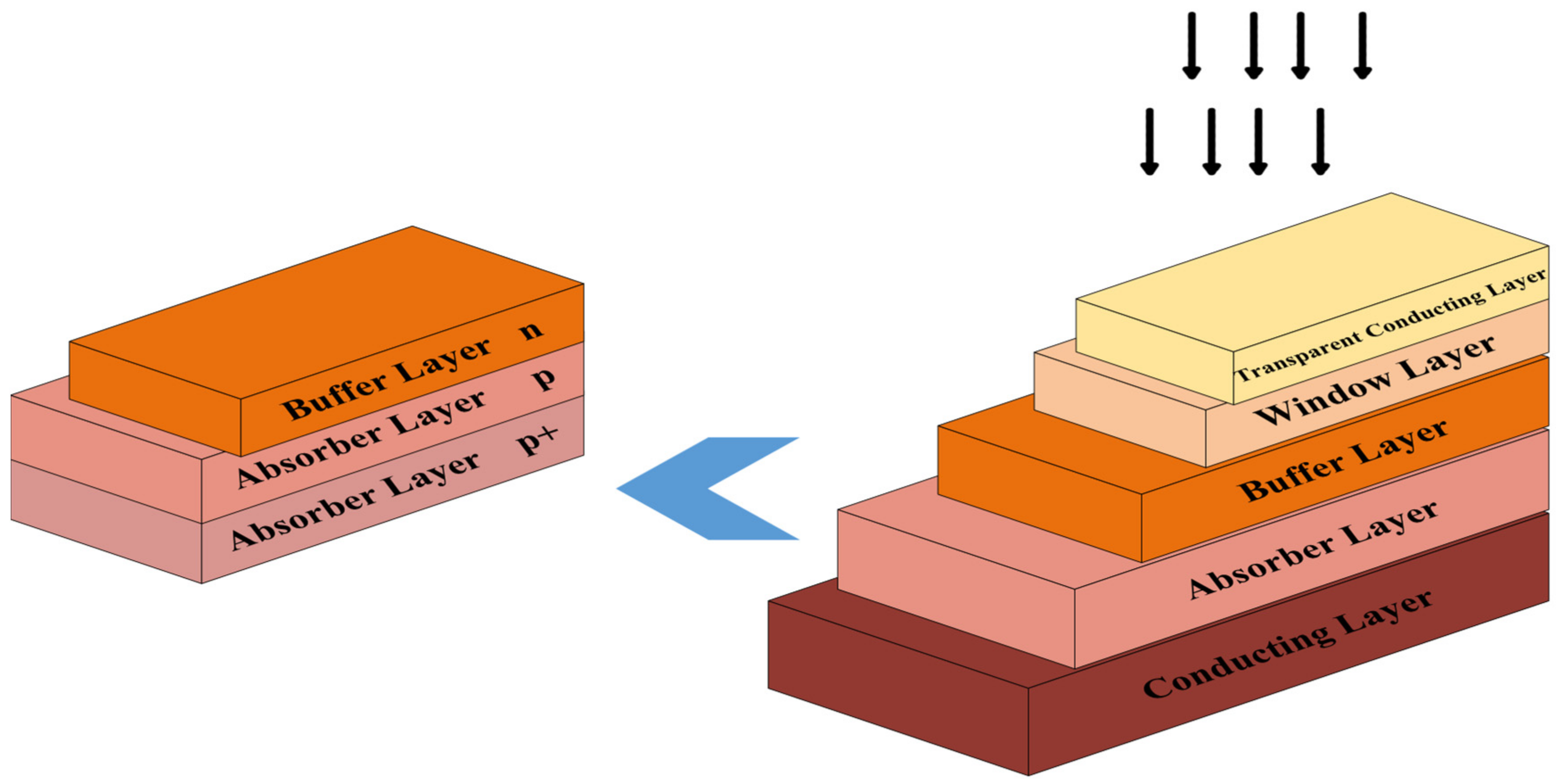
2. Modeling and Simulation for Material Selection

A regular structure was modeled for the CZTSe solar cell to analyze and investigate its performance. Figure 1 shows the schematic structure of the proposed solar cell. As illustrated in Figure 1, the CZTSSe-based solar cell structure consisted of different layers, in which CZTSe was used as the absorber layer. Based on the properties of CZTSe, it had an energy bandgap and absorption coefficient of over 1 eV and 104 cm−1, respectively [2]. In addition, the n-type window layer (such as ZnO) and the p-type absorber layer (CZTSe) formed a p-n junction. Likewise, the n-type cadmium sulphide (Cds) layer worked as a buffer layer. The front and back layers of the solar cell were indium tin oxide (ITO) transparent conducting layers and MO materials were employed as contacts in the proposed solar cell design. According to the properties of different materials, higher energy-band gap (Eg) materials such as window layers (the band gap of ZnO is over 3 eV) help more photons to easily reach the underlying layers. Thus, bandgap management is very important for obtaining better performance via the choosing of the best materials. The main idea of the buffer layer is to provide more routes for photons to be transmitted without being absorbed, to reduce defects in the absorber layer, and to align the energy bandgap between the absorber layer and window layer. Moreover, a molybdenum layer was used to increase light trapping and to reflect more photons back into the CZTSe layer. For the first step, using TCAD Silvaco software, an ATLAS code was prepared in order to build this structure—shown in Figure 1. Based on ref [2,5,31], materials were chosen and are detailed in Table 1.

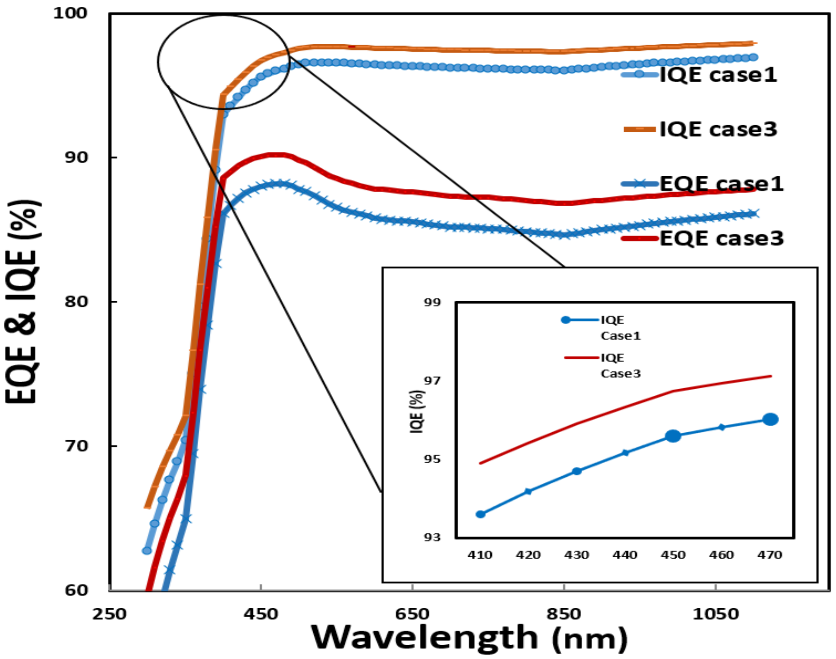
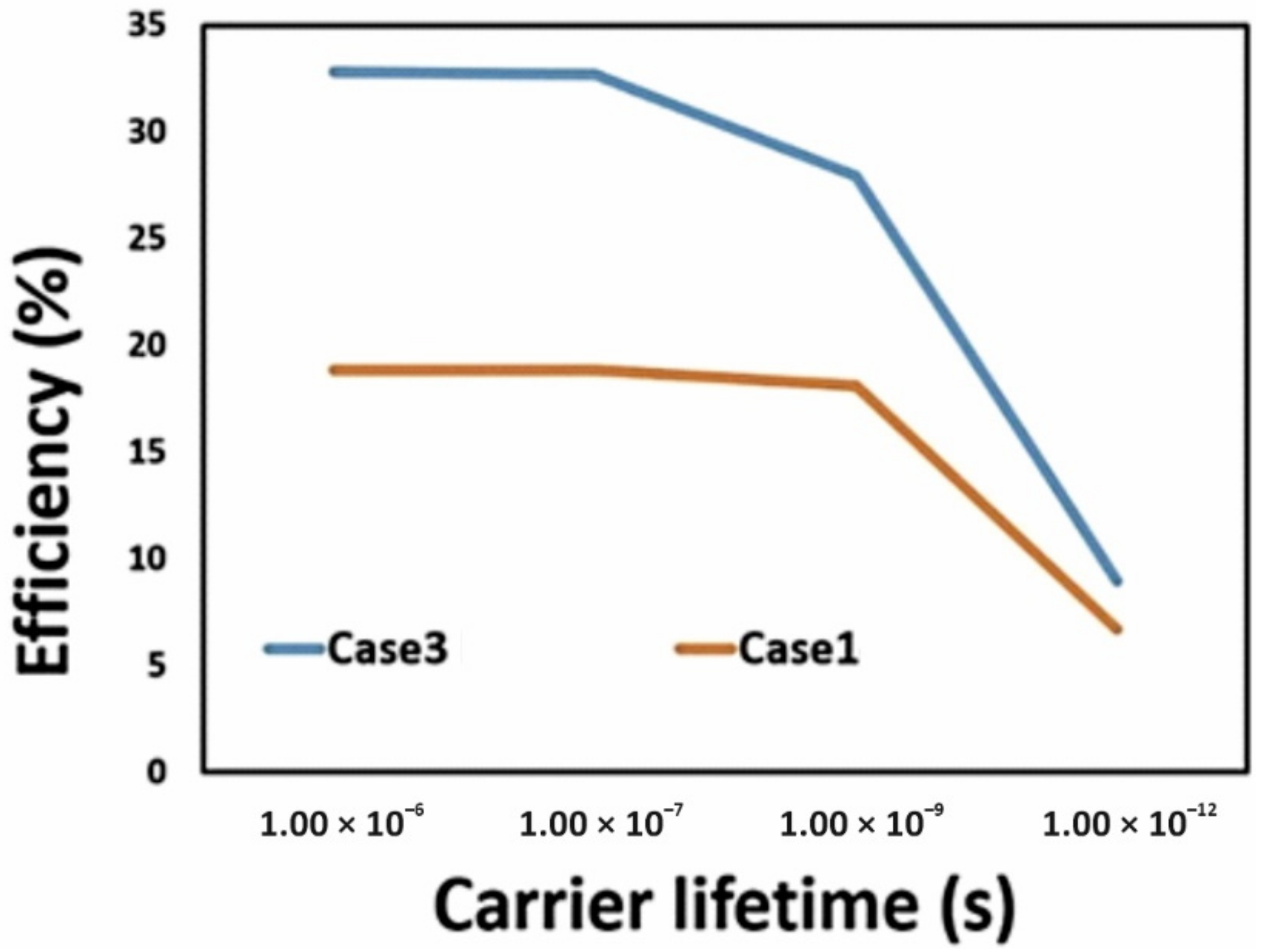
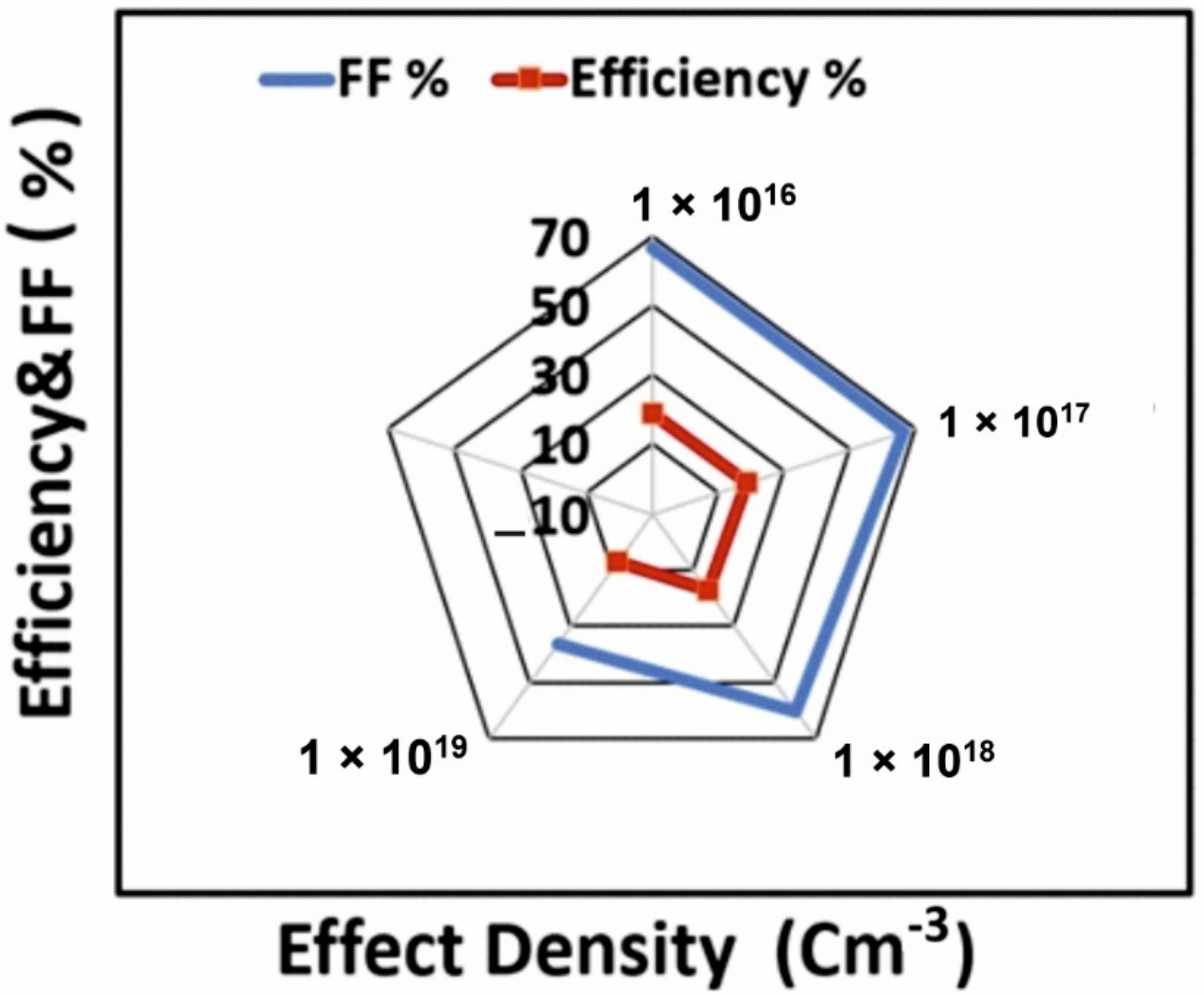
3. Results and Discussion

In this section, to perform the numerical simulations of the device characteristics, a Silvaco simulator was used to extract the electrical characteristics and optical behaviour of the proposed solar cell. Moreover, the impact of the carrier lifetime and thickness on the performance of the solar cell was studied. As shown in Table 2, different cases with different thicknesses and concentrations of ITO and absorber layers were analyzed. According to the efficiency results (shown in the tenth row of Table 1), by increasing the doping concentration of the absorber layer, the efficiency was significantly improved. Thus, in comparison to cases 1 and 2, where all parameters except the concentration were constant, increasing doping from 1 × 10¹⁵ to 1 × 10¹⁸ resulted in improved efficiency from 18.86% to 32%. Indeed, by increasing the doping concentration of the absorber layer (case 2), the width of the depletion region declined. Therefore, the short circuit current (Jsc) decreased slightly, since fewer carriers were collected at the contacts as a result of a reduction in carrier transmission. At the same time, the open circuit voltage (Voc) increased because of the lower recombination rate of the electron and holes than the rate in case 1, resulting in an amplification of the efficiency. More holes and fewer electrons in the absorber layer caused a change in the recombination rate. It is important to choose the doping concentration of the absorber precisely when the dopant concentration is so high, as more photons will be absorbed in the buffer layer instead of the absorber layer, and efficiency will be decreased. Higher doping concentrations lead to lower carrier mobility, higher leakage, and increased scattering. As such, the optimum doping concentration values were compared for different cases in Table 2.
In addition, by decreasing the thickness of the ITO layer and using the CSLO technique to make p+pn junction (case 3), the efficiency was again increased. Accordingly, it is believed that the efficiency of solar cells depends on the alignment band of the hetero-interface, and that the layer-thickness selection caused more light absorbance and less recombination of electrons and holes, as demonstrated in Table 2. Furthermore, the performance of the CZTS-based, Ge-based Cu2ZnGeSe4, and Si-based Cu2ZnSiSe4 Kesterite solar cells made with the proposed CSLO technique was analyzed. As illustrated in Table 2, the Ge-based Cu2ZnGeSe4 solar cell achieved the best optical and electrical results because of the Ge’s properties, such as having the best direct energy bandgap among the CZTS-based and Si-based Cu2ZnSiSe4 solar cells, providing an over 70 percent efficiency and fill factor, which represent the ratio of the maximum power to the minimum power (Pmin) and the ratio of the theoretical power to the maximum power (Pmax), respectively. Indeed, all of the mentioned parameters are essential for measuring the quality of solar cells. In Figure 2, the External Quantum Efficiency (the ratio of the anode current to the source photo current) and the Internal Quantum Efficiency (the ratio of the anode current to the available photo current) results versus wavelength (nm) for case 1 (without the CSLO technique) and case 3 (with the CSLO technique) are represented. Figure 2 shows that in case 3, by utilizing the proposed technique, the EQE was higher than conventional solar cells made without the CSLO technique. Firstly, it was obvious that the EQE and IQE were low at short wavelengths (λ); as the wavelength increased, they increased dramatically to reach their maximum values. Then, the IQE remained constant at mid-range wavelengths, in contrast to the EQE. The quantum efficiency variation versus different wavelengths was directly related to the number of input photons and their energy levels in comparison to the bandgap energy of the solar cell [32].
Figure 3 illustrates the spectral response of the proposed solar cell (case 3) against the wavelength. It is obvious that the available photo current and the cathode current differed from each other at lower wavelengths due to the lower numbers of photons, but at higher wavelengths, the trends looked like each other, and the cathode current was significantly increased. Furthermore, not only was the optical behavior considerably improved, but the electrical parameters were also increased by the CSLO technique.
Moreover, Table 3 illustrates a comparison of the hybrid structures, with those with that were combined with CZTSe-based solar cells having a higher efficiency than those without them. The hybrid structure with the Cu2ZnGeSe4 gained the maximum value of efficiency of 50.112% while the Si-based Cu2ZnSiSe4 obtained an efficiency of 33.61%, which was the lowest value. Similarly, Table 4 presents the comparison results of the proposed CZTSe-based solar cell made with the CSLO technique and other published papers with CZTSSe-based solar cells. By using the CSLO technique, the performance in comparison to conventional CZTSSe-based solar cells was significantly improved, yielding an efficiency of 32.6% and a fill factor of 79.55%.
In addition, the results of the efficiency variation versus carrier lifetime are depicted in Figure 4. As shown in Figure 4, the efficiency was increased as a result of an increase in carrier lifetime. The value of the carrier lifetime was chosen to be similar across different layers of the proposed solar cell (100 ns) over the entire simulation. Therefore, the carrier lifetime is an important parameter in solar cell design that affects the improvement of performance as well [36,37,38,39,40].
Subsequently, the impact of the absorber thickness on the electrical properties of the proposed solar cell for case 3 by increasing the p+ layer thickness when the width of the p region remained unchanged and the conventional case 1 were compared together as shown in Figure 5a. As demonstrated in Figure 5a, the Jsc varied constantly when changing the absorber layer from 1 µm to 4 µm (increased slightly), although the VOC was increased.
Moreover, by decreasing the absorber layer, the optical properties were decreased. As illustrated in Figure 5b, the EQE of the solar cell was decreased in lower wavelengths for case 1. Likewise, the electrical properties of case 1 declined by decreasing the width of the absorber layer, as demonstrated in Figure 5b. Thus, by selecting the optimum width of the absorber layer, more advantages will be obtained. In this regard, over the entire simulation, the optimum value of 2 microns was chosen for the absorber layer for the different cases.
Furthermore, another important parameter is the total effect density of the solar cell. Therefore, the effect densities of the p+pn junction and the ZnO/ITO layers must be selected precisely. Due to this, the effect density of the p+pn junction was chosen, as depicted in Table 1, to be consistent over the entire simulation, because the main of the purpose of this article was to study the effects of the proposed CSLO technique in carrier-generating layers. Furthermore, the impact of ZnO/ITO defect density was investigated. As shown in Figure 6, by changing the effect density from 1 × 1016 cm−3 to 1 × 1019 cm−3 for case 1, the efficiency and fill factor (%) decreased. Regarding this, the specifications of the layers must be considered in the simulation.
Modeling CZTSe solar cells in a simulated environment as presented here is critical for data analysis and real fabrication behavior projection. This optimization is beneficial for the commercial use of CZTSe solar cell technology. Various electrochemical and fabrication strategies are currently being researched in order to achieve layer specifications similar to those in Table 2. There are current results that suggest that the Pulsed laser deposition [41], Spray pyrolysis [42], Vacuum deposition method [43,44], Magnetron sputtering [45], and sol-gel [46,47] methods could be of use for achieving two divided absorber layers like those simulated by the CSLO technique.

4. Conclusions

In this work, the CSLO technique was introduced to improve the performance of CZTSe-based solar cells. Due to utilizing this technique, the efficiency and fill factor were increased by 12.76% and 13.74%, respectively; the electrical properties were improved as well. In addition, important parameters that affect the performance of the solar cell, such as the total effect density, carrier lifetime, and layer thickness, were investigated and simulated. Moreover, CZTS-based, Ge-based Cu2ZnGeSe4, and Si-based Cu2ZnSiSe4 Kesterite solar cells made with the proposed CSLO technique were simulated. According to the results, the efficiency was increased in each solar cell by employing the proposed technique. Furthermore, hybrid structures were compared. As represented here, by employing an CZTSe-based absorber layer with a CZTS, Cu2ZnGeSe4, and Si-based Cu2ZnSiSe4 one, the optical behavior and electrical property were remarkably improved. The optical behavior improvement was due to tuneable band gaps covering almost the entire solar spectrum and the high absorption coefficient.

Author Contributions

Conceptualization, S.R. and M.S.; methodology, S.R. and M.S.; software, S.R.; validation, S.R. and M.S.; formal analysis, S.R. and M.S.; investigation, S.R. and M.S.; resources, S.R. and M.S.; data curation, S.R.; writing—original draft preparation, S.R.; writing—review and editing, M.S.; visualization, S.R. and M.S.; supervision, M.S.; project administration, S.R. and M.S. All authors have read and agreed to the published version of the manuscript.

Funding

This research received no external funding.

Institutional Review Board Statement

Not applicable.

Informed Consent Statement

Not applicable.

Data Availability Statement

The data presented in this study are available from the corresponding authors upon reasonable request.

Conflicts of Interest

The authors declare no conflict of interest.

References

  1. Hong, F.; Lin, W.; Meng, W.; Yan, Y. Trigonal Cu2-II-Sn-VI4 (II = Ba, Sr and VI = S, Se) quaternary compounds for earth-abundant photovoltaics. Phys. Chem. Chem. Phys. 2016, 18, 4828–4834. [Google Scholar] [CrossRef] [PubMed]
  2. Adachi, S. Earth-Abundant Materials for Solar Cells: Cu2-II-IV-VI4 Semiconductors; John Wiley & Sons: Hoboken, NJ, USA, 2015. [Google Scholar]
  3. Altamura, G. Development of CZTSSe Thin Films based Solar Cells. Ph.D. Thesis, Université Joseph-Fourier—Grenoble I: Material Chemistry, Grenoble, France, 2014. [Google Scholar]
  4. Haque, K.; Baten, M.Z. On the prospect of CZTSSe-based thin film solar cells for indoor photovoltaic applications: A simulation study. AIP Adv. 2019, 9, 55326. [Google Scholar] [CrossRef] [Green Version]
  5. Mebelson, T.J.; Elampari, K. A study of electrical and optical characteristics of CZTSe solar cell using Silvaco Atlas. Mater. Today Proc. 2021, 46, 2540–2543. [Google Scholar] [CrossRef]
  6. Jiang, M.; Yan, X. Cu2ZnSnS4 thin film solar cells: Present status and future prospects. In Solar Cells—Research and Application Perspectives; Morales-Acevedo, A., Ed.; Intech: Rijeka, Croatia, 2013. [Google Scholar]
  7. Ratz, T.; Brammertz, G.; Caballero, R.; Leon, M.; Canulescu, S.; Schou, J.; Gütay, L.; Pareek, D.; Taskesen, T.; Kim, D.-H.; et al. Physical routes for the synthesis of kesterite. J. Phys. Energy 2019, 1, 42003. [Google Scholar] [CrossRef]
  8. Tumbul, A.; Aslan, F.; Göktaş, A.; Mutlu, I. All solution processed superstrate type Cu2ZnSnS4 (CZTS) thin film solar cell: Effect of absorber layer thickness. J. Alloys Compd. 2019, 781, 280–288. [Google Scholar] [CrossRef]
  9. Guerra, N.; Guevara, M.; Palacios, C.; Crupi, F. Operation and physics of photovoltaic solar cells: An overview. I + D Tecnológico 2018, 14, 84–95. [Google Scholar] [CrossRef]
  10. Attafi, D.; Boumaraf, R.; Meftah, A.; Sengouga, N. Effect of a Back-Surface Field and Passivation Layer on a Silicon Schottky Solar Cell. Trans. Electr. Electron. Mater. 2021, 22, 357–362. [Google Scholar] [CrossRef]
  11. Boukortt, N.E.I.; AlAmri, A.M.; Bouhjar, F.; Bouhadiba, K. Investigation and optimization of ultrathin Cu (In, Ga) Se2 solar cells by using silvaco-TCAD tools. J. Mater. Sci. Mater. Electron. 2021, 32, 21525–21538. [Google Scholar] [CrossRef]
  12. Luque, A.; Hegedus, S. Handbook of Photovoltaic Science and Engineering; John Wiley & Sons: Hoboken, NJ, USA, 2011. [Google Scholar]
  13. Jabbar, H.; Jeong, T. Ambient Light Energy Harvesting and Numerical Modeling of Non-Linear Phenomena. Appl. Sci. 2022, 12, 2068. [Google Scholar] [CrossRef]
  14. Dwivedi, D.K. Modeling of Photovoltaic Solar Cell Based on CuSbS2 Absorber for the Enhancement of Performance. IEEE Trans. Electron Devices 2021, 68, 1121–1128. [Google Scholar] [CrossRef]
  15. Antolin, E.; Zehender, M.H.; Garcia-Linares, P.; Svatek, S.A.; Marti, A. Considerations for the Design of a Heterojunction Bipolar Transistor Solar Cell. IEEE J. Photovolt. 2019, 10, 2–7. [Google Scholar] [CrossRef] [Green Version]
  16. Verma, M.; Routray, S.R.; Mishra, G. Analysis and optimization of BSF layer for highly efficient GaInP single junction solar cell. Mater. Today Proc. 2021, 43, 3420–3423. [Google Scholar] [CrossRef]
  17. De Rossi, F.; Taheri, B.; Bonomo, M.; Gupta, V.; Renno, G.; Nia, N.Y.; Rech, P.; Frost, C.; Cazzaniga, C.; Quagliotto, P.; et al. Neutron irradiated perovskite films and solar cells on PET substrates. Nano Energy 2021, 93, 106879. [Google Scholar] [CrossRef]
  18. Girish, K.; Vishnumurthy, K.; Roopa, T. Role of conducting polymers in enhancing the stability and performance of perovskite solar cells: A brief review. Mater. Today Sustain. 2022, 17, 100090. [Google Scholar] [CrossRef]
  19. Basumatary, P.; Agarwal, P. A short review on progress in perovskite solar cells. Mater. Res. Bull. 2021, 149, 111700. [Google Scholar] [CrossRef]
  20. Hayashi, Y.; Li, D.; Ogura, A.; Ohshita, Y. Role of i-aSi: H layers in aSi: H/cSi heterojunction solar cells. IEEE J. Photovolt. 2013, 3, 1149–1155. [Google Scholar] [CrossRef]
  21. Noge, H.; Saito, K.; Sato, A.; Kaneko, T.; Kondo, M. Two-dimensional simulation of interdigitated back contact silicon heterojunction solar cells having overlapped p/i and n/i a-Si: H layers. Jpn. J. Appl. Phys. 2015, 54, 8KD17. [Google Scholar] [CrossRef]
  22. Moulé, A.J.; Meerholz, K. Morphology Control in Solution-Processed Bulk-Heterojunction Solar Cell Mixtures. Adv. Funct. Mater. 2009, 19, 3028–3036. [Google Scholar] [CrossRef]
  23. Kumar, D.; Krishnan, N.S.; Ilango, M.S.; Ramasesha, S.K. Device simulations of a novel nanostructured CdS/CdTe solar cell with back contacts. J. Comput. Electron. 2021, 20, 324–329. [Google Scholar] [CrossRef]
  24. Ergen, O.; Celik, E.; Unal, A.H.; Erdolu, M.Y. Screen Engineered Field Effect Cu2O Based Solar Cells. IEEE Electron Device Lett. 2020, 41, 1138–1140. [Google Scholar] [CrossRef]
  25. Chee, K.W.; Hu, Y. Design and optimization of ARC less InGaP/GaAs single-/multi-junction solar cells with tunnel junction and back surface field layers. Superlattices Microstruct. 2018, 119, 25–39. [Google Scholar] [CrossRef]
  26. Hoehn, O.; Niemeyer, M.; Weiss, C.; Lackner, D.; Predan, F.; Franke, A.; Beutel, P.; Schachtner, M.; Müller, R.; Siefer, G.; et al. Development of Germanium-based wafer-bonded four-junction solar cells. IEEE J. Photovolt. 2019, 9, 1625–1630. [Google Scholar] [CrossRef]
  27. Trahms, M.; Jost, M.; Trinh, C.T.; Preissler, N.; Albrecht, S.; Schlatmann, R.; Rech, B.; Amkreutz, D. All-Thin-Film Tandem Cells Based on Liquid Phase Crystallized Silicon and Perovskites. IEEE J. Photovolt. 2019, 9, 621–628. [Google Scholar] [CrossRef]
  28. Paswan, S.K.; Chandra, D.; Bhatt, U.M.; Kumar, B. Performance Enhancement of CZTS and CZTSSe Solar Cells using CdS as Buffer Layer. In Proceedings of the 2020 International Conference on Electrical and Electronics Engineering (ICE3), Gorakhpur, India, 14–15 February 2020. [Google Scholar]
  29. Latrous, A.R.; Mahamdi, R.; Touafek, N.; Pasquinelli, M. Performance Enhancement in CZTS Solar Cells by SCAPS-1D. Int. J. Thin Film. Sci. Technol. 2021, 10, 1. [Google Scholar]
  30. Madan, J.; Pandey, R.; Sharma, R. Designing of CZTSSe Based SnS thin film solar cell for improved conversion efficiency: A simulation study with SCAPS. In Proceedings of the 2019 IEEE 46th Photovoltaic Specialists Conference (PVSC), Chicago, IL, USA, 16–21 June 2019. [Google Scholar]
  31. Bao, W.; Qiu, F.Y.; Bai, S.; Li, Y.; Chen, D.M. Study of band offset at ZnS/Cu2ZnIVS4 (IV = Si, Ge, Sn) heterointerfaces. Optoelectron. Adv. Mater. Rapid Commun. 2018, 12, 327–331. [Google Scholar]
  32. Braly, I.L.; de Quilettes, D.W.; Pazos-Outón, L.W.; Burke, S.; Ziffer, M.E.; Ginger, D.S.; Hillhouse, H.W. Hybrid perovskite films approaching the radiative limit with over 90% photoluminescence quantum efficiency. Nat. Photonics 2018, 12, 355–361. [Google Scholar] [CrossRef]
  33. Tripathi, S.; Maurya, S.; Kumar, B.; Dwivedi, D.K. Comparative analysis of CZTS/CZTSe/CZTSSe absorber layer for solar cell applications. In Proceedings of the 2020 International Conference on Electrical and Electronics Engineering (ICE3), Gorakhpur, India, 14–15 February 2020. [Google Scholar]
  34. Gohri, S.; Sharma, S.; Pandey, R.; Madan, J.; Sharma, R. Influence of SnS and Sn2S3 based BSF layers on the performance of CZTSSe solar cell. In Proceedings of the 2020 47th IEEE Photovoltaic Specialists Conference (PVSC), Calgary, AB, Canada, 15 June–21 August 2020. [Google Scholar]
  35. Vermang, B.; Ren, Y.; Donzel-Gargand, O.; Frisk, C.; Joel, J.; Salomé, P.; Borme, J.; Sadewasser, S.; Platzer-Björkman, C.; Edoff, M. Rear Surface Optimization of CZTS Solar Cells by Use of a Passivation Layer With Nanosized Point Openings. IEEE J. Photovolt. 2015, 6, 332–336. [Google Scholar] [CrossRef] [Green Version]
  36. Courel, M.; Andrade-Arvizu, J.A.; Vigil-Galán, O. The role of buffer/kesterite interface recombination and minority carrier lifetime on kesterite thin film solar cells. Mater. Res. Express 2016, 3, 95501. [Google Scholar] [CrossRef]
  37. Pandey, R.; Shimpi, T.; Munshi, A.; Sites, J.R. Impact of Carrier Concentration and Carrier Lifetime on MgZnO/CdSeTe/CdTe Solar Cells. IEEE J. Photovolt. 2020, 10, 1918–1925. [Google Scholar] [CrossRef]
  38. Shah, D.K.; Kc, D.; Muddassir, M.; Akhtar, M.S.; Kim, C.Y.; Yang, O.-B. A simulation approach for investigating the performances of cadmium telluride solar cells using doping concentrations, carrier lifetimes, thickness of layers, and band gaps. Sol. Energy 2021, 216, 259–265. [Google Scholar] [CrossRef]
  39. Shin, D.; Saparov, B.; Mitzi, D.B. Defect Engineering in Multinary Earth-Abundant Chalcogenide Photovoltaic Materials. Adv. Energy Mater. 2017, 7, 1602366. [Google Scholar] [CrossRef]
  40. Tampo, H.; Kim, K.M.; Kim, S.; Shibata, H.; Niki, S. Improvement of minority carrier lifetime and conversion efficiency by Na incorporation in Cu2ZnSnSe4 solar cells. J. Appl. Phys. 2017, 122, 023106. [Google Scholar] [CrossRef]
  41. Sun, R.; Zhuang, D.; Zhao, M.; Gong, Q.; Scarpulla, M.; Wei, Y.; Ren, G.; Wu, Y. Beyond 11% efficient Cu2ZnSn (Se, S)4 thin film solar cells by cadmium alloying. Sol. Energy Mater. Sol. Cells 2018, 174, 494–498. [Google Scholar] [CrossRef]
  42. Katagiri, H.; Jimbo, K.; Yamada, S.; Kamimura, T.; Maw, W.S.; Fukano, T.; Ito, T.; Motohiro, T. Enhanced Conversion Efficiencies of Cu2ZnSnS4-Based Thin Film Solar Cells by Using Preferential Etching Technique. Appl. Phys. Express 2008, 1, 041201. [Google Scholar] [CrossRef]
  43. Shooshtari, M.; Salehi, A. An electronic nose based on carbon nanotube -titanium dioxide hybrid nanostructures for detection and discrimination of volatile organic compounds. Sens. Actuators B Chem. 2022, 357, 131418. [Google Scholar] [CrossRef]
  44. Ge, J.; Yan, Y. Controllable Multinary Alloy Electrodeposition for Thin-Film Solar Cell Fabrication: A Case Study of Kesterite Cu2ZnSnS4. iScience 2018, 1, 55–71. [Google Scholar] [CrossRef] [Green Version]
  45. Tiwari, K.J.; Chetty, R.; Mallik, R.C.; Malar, P. Solid state synthesis and e-beam evaporation growth of Cu2ZnSnSe4 for solar energy absorber applications. Sol. Energy 2017, 153, 173–180. [Google Scholar] [CrossRef]
  46. Cazzaniga, A.; Crovetto, A.; Yan, C.; Sun, K.; Hao, X.; Estelrich, J.R.; Canulescu, S.; Stamate, E.; Pryds, N.; Hansen, O.; et al. Ultra-thin Cu2ZnSnS4 solar cell by pulsed laser deposition. Sol. Energy Mater. Sol. Cells 2017, 166, 91–99. [Google Scholar] [CrossRef] [Green Version]
  47. Agawane, G.L.; Vanalakar, S.A.; Kamble, A.S.; Moholkar, A.V.; Kim, J.H. Fabrication of Cu2 (ZnxMg1-x) SnS4 thin films by pulsed laser deposition technique for solar cell applications. Mater. Sci. Semicond. Process. 2018, 76, 50–54. [Google Scholar] [CrossRef]
Figure 1. Schematic of the proposed CZTSe-based solar cell structure.
Applsci 12 04119 g001
Figure 2. EQE and IQE vs. optical wavelength for case 1 and case 3.
Applsci 12 04119 g002
Figure 3. Available photo current and cathode current versus optical wavelength for case 3.
Applsci 12 04119 g003
Figure 4. Efficiency variation versus carrier lifetime.
Applsci 12 04119 g004
Figure 5. (a) Electrical properties versus absorber thickness. (b) EQE versus absorber thickness for Case 1.
Applsci 12 04119 g005
Figure 6. Efficiency and FF versus effect density for case 1.
Applsci 12 04119 g006
Table 1. Standard material parameters used in the solar cell design shown in Figure 1.
ParametersCu2ZnSiSe4Cu2ZnGeSe4CZTSCZTSeCdSZnOITO
Band gap (eV)32.11.51.042.43.33.6
Electron affinity (eV)2.43.44.14.154.54.64.2
Dielectric permittivity7.56.871010910
Electron mobility (cm2/Vs)606060100100100100
Hole mobility (cm2/Vs)20202025101010
Effective conductance band density (cm/s)2.2 × 1018
Effective valence band density (cm/s)1.8 × 1019
Defect density (cm−3)1 × 10131 × 10131 × 10131 × 10136 × 1016--
Table 2. Thickness (T) micro meter and doping concentration (C)-change results.
Case 1Case 2Case 3-CSLOCase 4-CSLOCase 5-CSLOCase 6-CSLO
MaterialTCTCTCTCTCTC
ITO0.031 × 10190.031 × 10190.021 × 10190.021 × 10190.021 × 10190.021 × 1019
ZnO0.081 × 10180.081 × 10180.081 × 10180.081 × 10180.081 × 10180.081 × 1018
CdS0.031 × 10170.031 × 10170.031 × 10170.031 × 10170.031 × 10170.031 × 1017
CZTSe (Cu2ZnSnSe4)21 × 101521 × 10180.5
1.5
1 × 10¹⁶
1 × 10¹⁹
------
Cu2ZnSnS4------0.5
1.5
1 × 10¹⁶
1 × 10¹⁹
----
Cu2ZnSiSe4--------0.5
1.5
1 × 10¹⁶
1 × 10¹⁹
--
Cu2ZnGeSe4----------0.5
1.5
1 × 10¹⁶
1 × 10¹⁹
Efficiency (η%)18.863232.666862.3170.64
Voc (v)0.3780.5480.5370.991.21.31
Jsc (A/cm2)0.0740.0730.0760.0780.0740.075
Fill Factor (%)66.7979.4479.5586.0369.7371.67
Pmax (W)0.0180.0320.03260.0680.0620.07
Table 3. Comparation results of hybrid solar cells.
Solar CellFill Factor (%)Efficiency (%)
hybrid structure (CZTSe and CZTS)6641.54
hybrid structure (CZTSe and Cu2ZnSiSe4)4233.61
hybrid structure (CZTSe and Cu2ZnGeSe4)54.8250.112
Table 4. Comparation results of the proposed solar cell with previously published solar cells.
ReferenceFill Factor (%)Efficiency (%)
Conventional CZTSe solar cell (Case 1)66.7918.86
Case 379.5532.6
[33]38.24.35
[34]76.4617.04
[35]50.8 ± 4.15.5 ± 0.6
Publisher’s Note: MDPI stays neutral with regard to jurisdictional claims in published maps and institutional affiliations.

