Article

Influence of Grid Aperture Ratio on Electron Transmittance and Electron Beam Spot Size in Field Emission Processes of Carbon Nanotubes

1
School of Instrument Science and Engineering, Southeast University, Nanjing 210096, China
2
CAS Key Laboratory of Nanophotonic Materials and Devices, CAS Key Laboratory of Standardization and Measurement for Nanotechnology, CAS Center for Excellence in Nanoscience, National Center for Nanoscience and Technology, Beijing 100190, China
3
China Ship Scientific Research Center, Wuxi 214082, China
*
Authors to whom correspondence should be addressed.
These authors contributed equally to this work.
Appl. Sci. 2024, 14(8), 3311; https://doi.org/10.3390/app14083311
Submission received: 18 March 2024 / Revised: 9 April 2024 / Accepted: 12 April 2024 / Published: 15 April 2024
(This article belongs to the Section Nanotechnology and Applied Nanosciences)

Abstract

:
Field emission is an important work mode for electron sources, and carbon nanotubes (CNTs) have been extensively studied for their good emission properties. It is well known that the parameters of the grid deeply influence the field emission performance of CNTs, a relationship that requires further elucidation. Therefore, in this study, the relationship between the grid aperture ratio and electron transmittance was studied through simulations and experiments. This study’s results indicate that the electron transmittance improved as the grid aperture ratio increased. Meanwhile, electron beam spot simulations and imaging experiments indicate that an increased grid aperture ratio will expand the cathode electron divergence, leading to a larger electron beam spot size. These results demonstrate that there is a trade-off in maintaining the grid aperture ratio between high electron transmittance and relatively small electron beam spot size, and the optimum grid aperture ratio is between 75% and 85%. These results will provide a reference for the design and optimization of X-ray tubes and other electron sources.

1. Introduction

The X-ray has been widely used in medical diagnosis, security checks, and drug testing since Roentgen discovered it in 1895 [1]. It has made remarkable progress in communication, material analysis, high-resolution imaging, and other fields [2,3,4,5]. X-ray sources can be roughly classified into two types: thermal cathodes and cold cathodes. Traditional thermal cathode X-ray sources exhibit limitations such as low current densities, high operating temperatures, and long response times, which render them unsuitable for miniaturization. Moreover, high-power operations can lead to material degradation and shorten the working lifespans of devices [6,7,8]. On the contrary, cold cathode X-ray sources are based on the principle of field emission; when the cathode surface is subjected to a strong electric field, electrons can break through the potential barriers and escape, and electrons bombard the anode metal to produce X-rays. This type of X-ray source exhibits good real-time performance, low power consumption, and easy integration [9,10,11,12,13,14].
Many materials have been tried as cold cathodes. Specifically, carbon nanotubes (CNTs) have attracted much attention due to their excellent thermal properties, large aspect ratio, high electrical conductivity, and mechanical stability [15,16,17,18,19]. Compared to other cathode materials, they can be easily made into various shapes of emitters by patterned growth, making them a popular choice for cathodes in vacuum devices [20,21,22,23,24]. Some reports have explored the applications of CNTs such as X-ray microscopes [25], portable X-ray systems [26], cathode ray tube type lighting elements, and vacuum fluorescence display panels [27]. The field emission performance of CNTs is relatively stable, and their manufacturing process has gradually developed.
It is well known that a gate electrode is necessary during CNT field emission processes to control and modulate the emission current [28,29,30,31]. A change in the gate voltage alters the distribution of the electric field between the gate and the cathode electrodes, causing variations in the field emission current of CNTs. Many studies have been conducted on gate electrodes to improve field emission performance. The effects of concave grids on field emission properties were investigated in [32]. The effects of the grid aperture ratio and the relative position between the cathode and gate on field emission performance were explored in [33]. Achieving digital control of miniature X-ray tubes using a focusing-functional gate was accomplished in [34]. The influence of the alignment and dislocation relationship between the grid and cathode on electron transmittance was studied in [35]. A grid structure combining coarse and fine grids was designed to enhance the cathode current in [36]. The leakage current was reduced and the transmission ratio was improved through the self-aligned structure of the gate and CNTs in [37]. Based on point-like CNTs, the focusing effect of the electron beam spot through indium tin oxides (ITOs) glass was tested in [38]. Our team has previously reported on some papers in the field of CNT field emission, including the production of CNTs of various morphologies, the enhancement of the stability of CNTs, and the application and design of cold cathode X-ray tubes [39,40,41]. In the process of designing X-ray tubes based on CNTs, we found that the gate not only affects the electron transmittance but also the divergence of the electron beam, which affects the performance of the X-ray tube. However, previous reports have mainly focused on improving the electron transmittance of the grid, and research on the influence of the grid on the electron beam spot is lacking. Therefore, this paper presents a study on the grid aperture ratio.
In actual experiments, different grid aperture ratios can change the electric field distribution on both sides of the grid, impacting the current of each electrode, electron transmittance, and electron beam spot size. Therefore, in this study changes in electrode current, electron transmittance, and electron beam spot size caused by variations in the grid aperture ratio were analyzed through simulations and field emission experiments. In addition, fluorescence imaging experiments were performed on the grid, and the simulation results were combined to explore the influence of different voltages and grid aperture ratios on the size of the electron beam spot. The conclusions in this paper will be useful for the design of cold cathode electron sources such as X-ray tubes and travelling-wave tubes.

2. Experimental Section

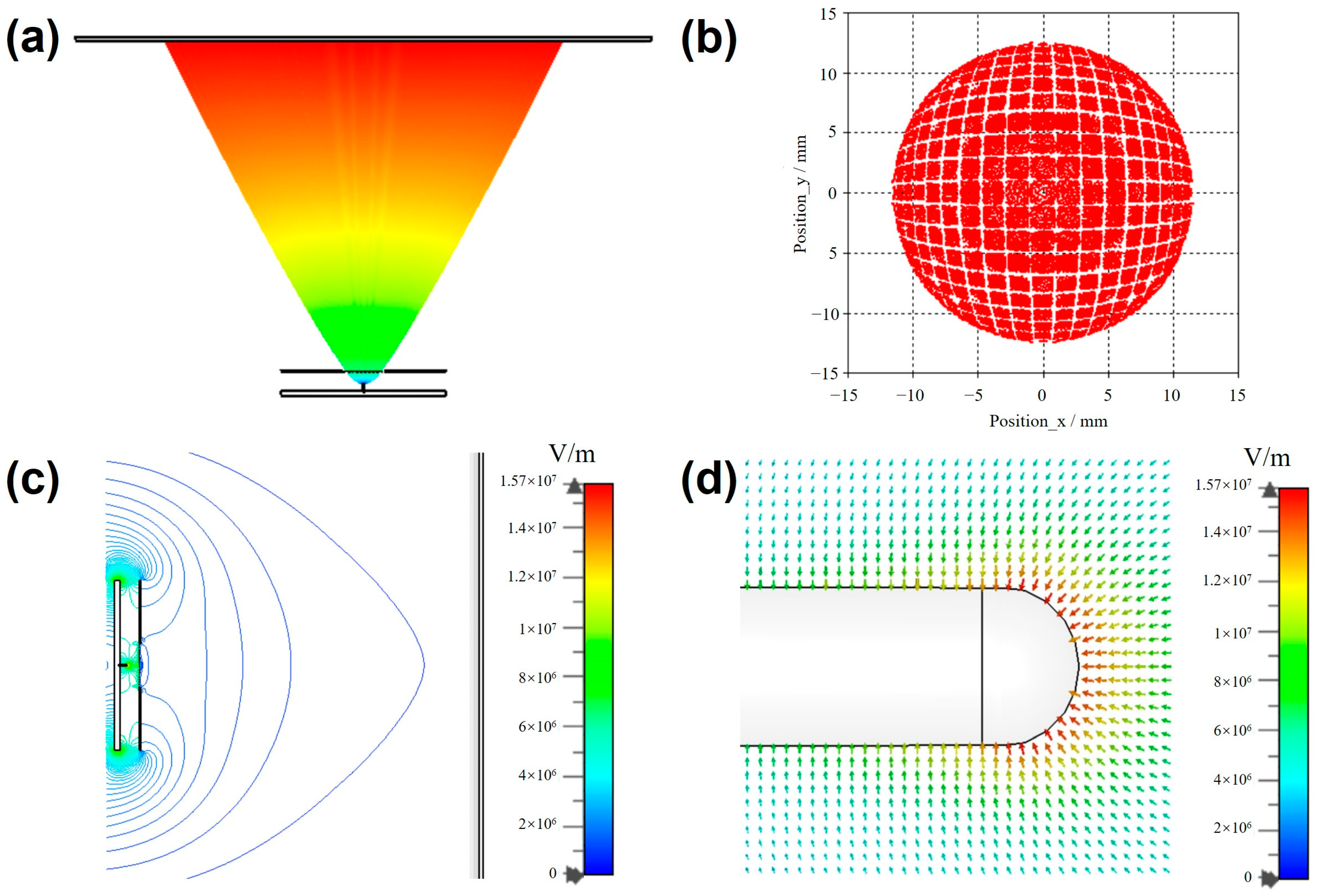
2.1. Simulation of the Field Emission Model

The field emission model was simulated using CST Studio Suite 2020 (CST). CST is an electromagnetic simulation software developed by the French Dassault Systemes. The trajectory and distribution of electrons under the action of the electric field in all space can be obtained by CST simulation [42]. Figure 1a shows the electron emission process based on CNTs cathode. A metal grid mesh with square grid holes was set between the anode and cathode. The width of the grid wire is represented by W, and the distance between the wires is represented by Wd, as depicted in Figure 1c. Electrons emitted from the cathode could traverse the grid holes and reach the anode plate, constituting the anode current. The ratio of anode current to cathode current was defined as electron transmittance. The formula for defining the aperture ratio is as follows:
A p e r t u r e   R a t i o = W d 2 × 100 % W d + W 2
The initial parameter values of the specific structure in the CST model are presented in Table 1. According to the system parameter values in Table 1, the size of the cell, iteration number, relative accuracy, and other parameters can fully make the simulation results have a high simulation accuracy. The cathode–gate distance and gate–anode distance values of the current model can enlarge the area of the electron beam spot. The voltages and the distance between the grid wires are the key parameters that were varied in the simulation. Initially, the anode voltage was held constant at 7.0 kV, and the gate voltage was set to 3.0 kV to simulate and test the grid with various aperture ratios. The grid wire width was fixed at 20 μm, while the distance between the wires was incrementally increased to achieve an aperture ratio ranging from 11% to 94%. In the simulation, we mainly investigated the current change for each electrode under different conditions, changes in electron transmittance, and the size of the electron beam spot.

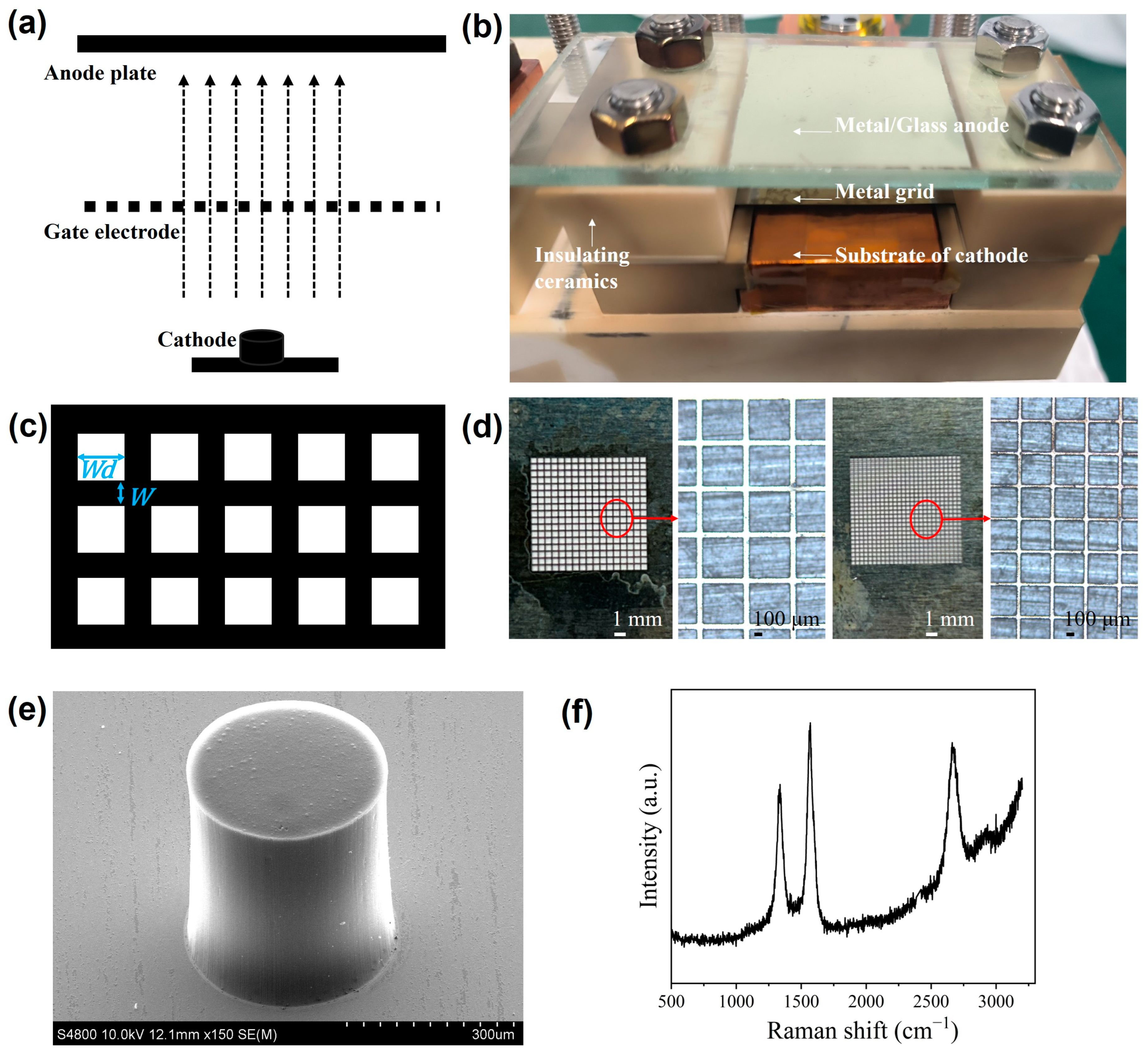
2.2. Field Emission Measurements with Triode Structures

The experiments were conducted using triode field emission structures under a vacuum degree of 5 × 10⁻⁸ mbar. The field emission experimental setup is shown in Figure 1b, which includes the carbon nanotube cathode and substrate, a metal gate, and an anode plate. Compared to most diode measurement structures, the experimental setup in Figure 1b can measure both the electron transmittance and the size of the electron beam spot. Figure 1d shows some of the metal grids used in the experiments, and these stainless-steel grids had been laser machined. The grids are smooth and flat. As shown in Figure 1e, the cathode used in the experiment is a multi-walled CNT film. Figure 1f shows the Raman spectrum of the cathode, indicating that the CNTs contain very few defects. The distance between each electrode was adjusted by insulating ceramic pads of different thicknesses. Firstly, to maintain good insulation, a 20 μm wide grid wire was used, and the distance between grid wires was increased from 40 μm to 370 μm while maintaining the anode voltage at 7.0 kV and the gate voltage at 3.0 kV. Secondly, a width of 30 μm, a wire distance of 275 μm, and a grid with an aperture ratio of 81.3% was used. The gate voltage was maintained at 3.7 kV, and the anode voltage was gradually raised from 0 V to 7.0 kV. Finally, the anode voltage was kept at 7.0 kV, while the gate voltage was kept at 3.6 kV, and the grid wire width and grid wire distance were varied to achieve a grid aperture ratio of 70%.

2.3. Fluorescence Imaging Experiments

In addition, fluorescence imaging experiments of electron beam spots were conducted. The experimental setup used in the fluorescence imaging experiment is shown in Figure 1b. The metal anode was replaced with an ITO anode, while the other structures remained unchanged. To explore the changing pattern of the electron beam spot, an ITO rectangular conductive glass plate was utilized as the anode, and CNTs were used as the cathode emitter. The gate was composed of a metal grid with a grid wire width of 20 μm and a grid wire distance of 50 μm. The lower surface of the glass plate was uniformly coated with fluorescent powder for imaging. Fluorescence imaging experiments were performed at different anode voltages, different gate voltages, and different aperture ratios.

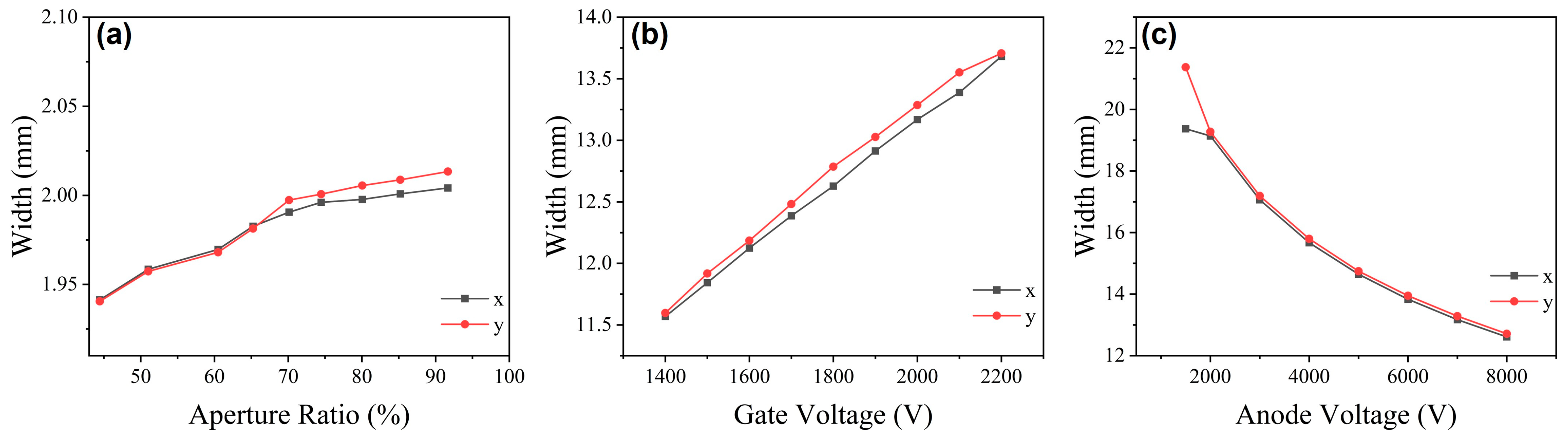
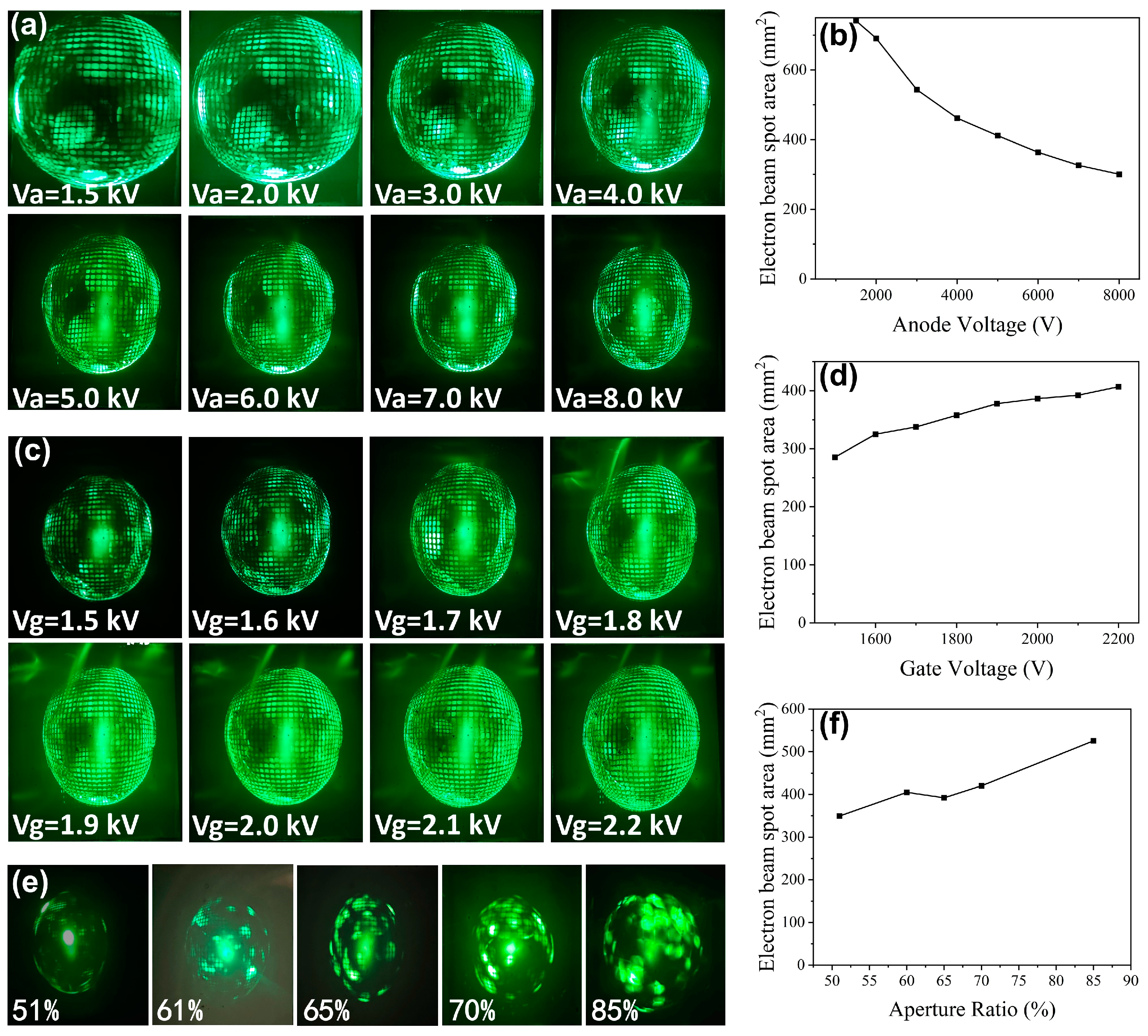
3. Results and Discussion

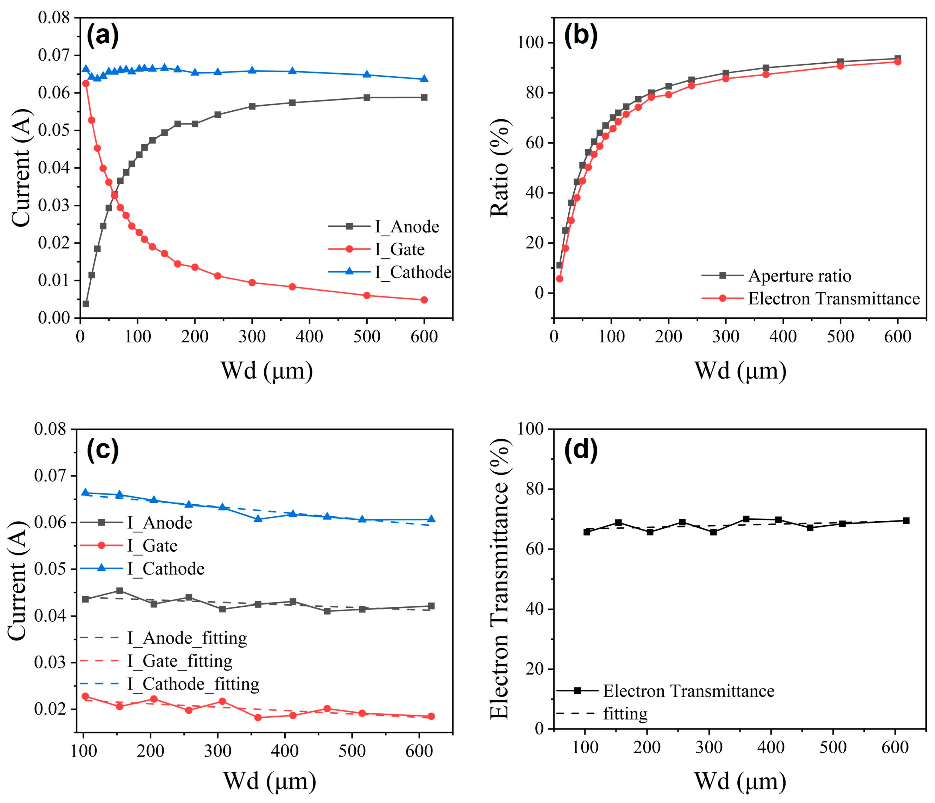
3.1. The Results of the Triode Field Emission Structure Simulation

In this section, the electron transmittance simulation results are discussed. Figure 2 is a schematic diagram of the CST simulation results. Figure 2a shows the flight trajectory of the electrons. Figure 2b shows the electron distribution on the anode plate. The red part in Figure 2b shows the distribution of electrons, while the white part indicates that some electrons have been intercepted by gate. Figure 2c shows the electric field intensity distribution of the model in space, and Figure 2d shows the electric field direction at the emission tip of the cathode. The electric field intensity on the surface of the cathode tip is the highest. The flight trajectory of electrons only depends on the electric field intensity in space.
Figure 3a illustrates the variation in electrode current at different grid wire distances. Figure 3b displays the trends in electron transmittance and grid aperture ratio at varying grid wire distances. The simulation results revealed that as the aperture ratio increased, the cathode current initially decreased, followed by an increase and then another decrease. When the distance between the grid wires was between 10 μm and 30 μm, the cathode current gradually decreased due to the broader grid wires, resulting in the grid wire intercepting most of the electrons. From 30 μm to 147 μm, the cathode current increased gradually because the electric field distribution between the cathode and grid altered with increasing grid wire distance, enhancing the tunneling ability of electrons and enabling more significant emission from the cathode. However, from 147 μm to 600 μm, the cathode current gradually declined as the effective projection area of the grid wire on the cathode decreased rapidly, weakening the cathode surface electric field and diminishing the field emission capacity, so the cathode current gradually tended to decrease. Due to the reduction in the number of electrons intercepted by the grid wire, the gate current decreased gradually while the anode current increased, ultimately approaching saturation. The trends in electron transmittance correspond to the variation in grid aperture ratio, increasing gradually with an increase in the grid aperture ratio.
Figure 3c depicts the current variations in each electrode at varying grid wire distances. Figure 3d shows the changes in electron transmittance at different grid wire distances. The grid wire width was set to 20 μm, while the anode voltage, gate voltage, distance between the grid and cathode, and distance between the grid and anode were fixed at 7.0 kV, 3.0 kV, 700 μm, and 2.0 cm, respectively. The gate voltage and anode voltage were kept constant, while the width of the grid wire and the distance between the grid wires were adjusted to achieve an aperture ratio of 70%. The anode current decreased from 0.0434 A to 0.0422 A, the gate current decreased from 0.0228 A to 0.0185 A, and the cathode current decreased from 0.0664 A to 0.0607 A. As shown in Figure 3c, linear function fitting was performed, and these results showed that the current of each electrode decreased with increasing grid wire distance. The linear fitting curve in Figure 3d revealed that the electron transmittance remained between 65% and 70% with a slight increase. The simulation results indicate that although the aperture ratio remained constant, the current in each electrode decreased, and the electron transmittance slightly increased.
In addition, the simulation results of the electron beam spot were analyzed. Figure 4a shows the simulation results. The voltage was kept constant, and the width of the grid wire was set at 20 μm. The distance between the grid wires was gradually increased, and grids with different aperture ratios were simulated. A particle monitor was set up on the gate surface near the cathode, which then calculated the electron beam spot size in the x and y directions. When the aperture ratio increased from 44% to 90%, the electron beam spot size in both the x and y directions increased. Specifically, the electron beam spot size in the x direction increased from 1.9413 mm to 2.0042 mm, while the electron beam spot size in the y direction increased from 1.9405 mm to 2.0134 mm. As the aperture ratio of the grid increased, the size of the electron beam spot gradually increased. The electric field intensity on the tip of the cathode was higher, and the ability of electrons to emit from the side was enhanced, increasing the electron beam spot size.
At last, the width of the grid wire was set to 20 μm, and the distance between the grid wires was set to 50 μm. We set up a particle monitor on the surface of the anode. Figure 4b,c show the relationship between the size of electron beam spots and voltage when only increasing the gate voltage and anode voltage. The simulation results showed that when the gate voltage increased from 1.4 kV to 2.2 kV, the width of the electron beam spot in the x direction increased from 11.5686 mm to 13.6816 mm and the width of the electron beam spot in the y direction increased from 11.5973 mm to 13.7069 mm. As the gate voltage increased, the field emission capability of the cathode increased and more electrons were emitted, leading to an increase in the electron beam spot size. When the anode voltage increased from 1.5 kV to 8.0 kV, the width of the electron beam spot in the x direction decreased from 19.3699 mm to 12.6113 mm and the width of the electron beam spot in the y direction decreased from 21.37351 mm to 12.7133 mm. The variation trend of the electron beam spot in the x and y directions remained consistent. An increase in anode voltage shortened the time of flight of the electrons, thereby reducing the electron beam spot size. Therefore, changing the gate voltage and anode voltage affected the size of the electron beam spot.

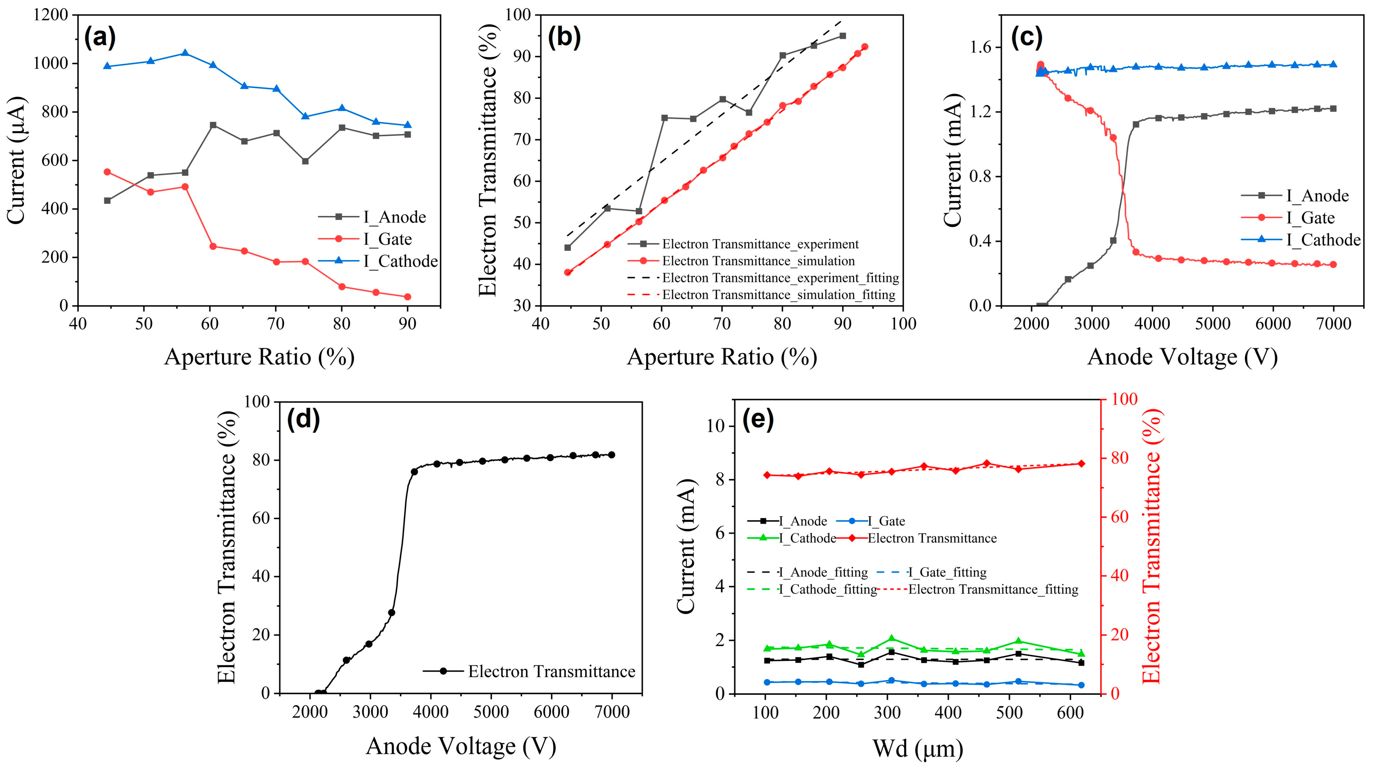
3.2. The Electron Transmittance Measurements

The results of electron transmittance field emission experiments are analyzed in this section. The change trend of the electrode current is shown in Figure 5a, and the change trend of electron transmittance is shown in Figure 5b. As shown in Figure 5a, when the grid aperture ratio increased from 44% to 56%, there was a slight increase in cathode current. The increase in the aperture ratio enhanced the electric field at the cathode surface. However, the cathode current decreased continuously as the aperture ratio increased from 56% to 90%. As the distance between the gate filaments increased, the number of electrons intercepted by the gate filaments decreased, the gate current decreased, and the projected area of the gate filaments on the cathode decreased. As a result, the excitation ability of the electric field to the electrons was weakened, leading to a reduction in the field emission current. As the gate current decreased, the anode current increased, resulting in a continuous increase in electron transmittance. When the grid aperture ratio reached 60%, the anode current decreased and gradually became saturated. After the grid aperture ratio was greater than 75%, the current intercepted by the gate also gradually became saturated, and the electron transmittance increased significantly. Figure 5b shows the trend of the electron transmittance with the grid aperture ratio in both the experiments and simulation. The error of electron transmittance between simulation and actual testing was due to the actual grid aperture ratio being greater than the design value. The grid wire may melt during laser processing, causing the actual width of the grid wire to be smaller than the design value, resulting in an actual grid aperture ratio greater than the design value. Therefore, the experimental electron transmittance was higher than that in simulation. Although there were some differences between experiment and simulation, the linear fitting curves revealed that the electron transmittance and the grid aperture ratio approximate a linearly increasing relationship.
The currents of three electrodes at different anode voltages are shown in Figure 5c, and the corresponding electron transmittance is plotted in Figure 5d. The grid aperture ratio and gate voltage were kept constant. As shown in Figure 5c, both anode current and electron transmittance were minimal at a low anode voltage. The cathode current remained essentially constant as the anode voltage increased. However, as the anode voltage approached the gate voltage, a significant number of electrons were propelled through the grid hole by the high-voltage electric field and reached the anode, rapidly increasing both the electron transmittance and anode current. Upon reaching 3.7 kV, the anode current approached saturation, indicating that further increases in voltage had little impact on the field emission current of the cathode. Nevertheless, an increase in the anode voltage resulted in a higher anode current and electron transmittance. Overall, these findings demonstrated that when the gate voltage was held constant, the anode voltage had minimal influence on the emission current of the cathode field. However, a higher anode voltage could enhance the electron transmittance and anode current.
Although the aperture ratio was unchanged, the increase in grid wire distance was more significant than the increase in grid wire width. Figure 5e shows the variation in the currents and electron transmittance as the grid wire distance increased. Figure 5e indicated that the currents at all electrodes decreased slightly as the grid wire distance increased. Figure 5e also showed that as the grid wire distance increased from 103 μm to 618 μm, the electron transmittance only slightly increased from 74.6% to 78.5%, with the electron transmittance essentially remaining around 76%. This minimal increase in electron transmittance was attributed to the reduced number of electrons captured by the grid wire. Thus, the electron transmittance remained essentially constant despite the increase in grid wire distance. The grid aperture ratio determined the electron transmittance. When the grid aperture ratio increased, electron transmittance also increased, and when the grid aperture ratio remained constant, electron transmittance also remained almost constant. Therefore, the grid aperture ratio determined the electron transmittance.

3.3. The Electron Beam Fluorescence Imaging Experiments

To study the variation in electron beam spot size at different aperture ratios, fluorescence imaging experiments were conducted. The gate voltage was maintained at 1.6 kV while the anode voltage was increased from 1.5 kV to 8.0 kV. The fluorescence images obtained are shown in Figure 6a. Figure 6b illustrates the relationship between the electron beam spot size and the anode voltage. The y-axis of Figure 6b represents the area of the electron beam spot. As the voltage increased, the area gradually decreased, and the electron beam spot narrowed inward. This phenomenon was attributed to the enhancement of the anode electric field, which reduced the time for electrons to reach the anode. It took less time for the electrons to spread around, and the electron beam became more concentrated. As a result, the electron beam spot on the anode was reduced.
When the anode voltage was kept constant at 7.0 kV and the gate voltage was increased from 1.7 kV to 2.2 kV, a fluorescence image was produced, as shown in Figure 6c. The relationship between the electron beam spot size and the gate voltage is illustrated in Figure 6d. With an increase in the gate voltage, the area of the electron beam spot on the fluorescent plate gradually expands. This indicates that, under fixed anode voltages, an increase in gate voltage leads to a more significant emission of electrons from the cathode, resulting in an expansion of the electron beam’s divergence angle.
Figure 6e shows the fluorescent images at different aperture ratios. Figure 6f shows the area of the electron beam spot at different aperture ratios. The voltage of each electrode is unchanged, and it can be observed that an increase in the aperture ratio intensifies the divergence of cathode electrons, thus increasing the size of the electron beam spot, which is not conducive to subsequent focusing. Therefore, it is only possible to increase the aperture ratio of the grid with limitations.
To summarize the work described above, from the simulation and experiment results, with an increase in the grid aperture ratio, the cathode current increased first and then decreased, the gate current decreased continuously, and the anode current increased until saturation when the anode voltage and the gate voltage remained constant. The electron transmittance increased as the aperture ratio increased. When the gate voltage was fixed and the grid aperture ratio remained constant, the cathode current remained stable. The higher the anode voltage, the greater the anode current and electron transmittance. Furthermore, if the anode voltage and gate voltage remained constant, the current of each electrode decreased as the gate distance increased, while the electron transmittance remained stable. Increasing the anode voltage could reduce the electron beam spot size, enhancing the electron transmittance. While increasing the gate voltage increased the cathode current, it also enlarged the size of the electron beam spot. Increasing the grid aperture ratio elevated the electron transmittance. However, it also caused a reduction in the field emission current of the cathode, and the electron divergence of the cathode increased. The electron transmittance was still low when the grid aperture ratio was less than 75%. When the aperture ratio was greater than 85%, the electron transmittance was saturated but exacerbated the electron beam dispersion, and the size of the anode electron beam spot also gradually increased.

4. Conclusions

These results indicated that the electron transmittance of CNT triode field emission structures was determined by the aperture ratio of the grid. A larger aperture ratio of the grid resulted in higher electron transmittance; however, it also caused the cathode electron divergence to increase, resulting in an enlarged electron beam spot size. It was necessary to strike a balance between electron transmittance and the size of the electron beam spot rather than barely increase the grid aperture ratio. For the CNT triode field emission structure described in this work, to obtain a large anode current and small electron beam divergence, achieving a trade-off between high electron transmittance and small electron beam spot size, the aperture ratio of the grid can be kept between 75% and 85%. Compared with existing reports, this study not only presents high electron transmittance but also achieved a balance between electron transmittance and electron beam spot size. This study, which focused on determining the optimal grid aperture ratio for achieving a balance between transmittance and electron divergence, could provide a reliable reference for applications related to cold cathode X-ray tubes.

Author Contributions

Conceptualization, Y.L. (Yongbo Li) and Z.L.; data curation, X.L. and X.S.; formal analysis, X.L.; funding acquisition, S.F., Z.L. and L.Z.; investigation, A.W., K.C. and S.Z.; methodology, Y.L. (Yuanxun Li) and X.L.; project administration, S.F., Z.L. and L.Z.; resources, Z.L. and L.Z.; software, Y.L. (Yuanxun Li); supervision, C.L.; validation, X.S.; writing—original draft, Y.L. (Yongbo Li); writing—review and editing, Z.L. All authors have read and agreed to the published version of the manuscript.

Funding

This work was supported by the National Key R&D Program of China (Grant No. 2021YFC2802000), Natural Science Foundation of China (Grant Nos. 52372141, 52072084, 51925203, 52222207), Strategic Priority Research Program of Chinese Academy of Sciences (Grant No. XDB36000000), and Key Area Research and Development Program of Guangdong Province (Grant No. 2020B0101020002).

Institutional Review Board Statement

Not applicable.

Informed Consent Statement

Not applicable.

Data Availability Statement

The data presented in this study are available on request from the corresponding authors.

Conflicts of Interest

The authors declare no conflicts of interest.

References

  1. Röntgen, W.C. On a new kind of rays. Science 1896, 3, 227–231. [Google Scholar] [CrossRef] [PubMed]
  2. Parmee, R.J.; Collins, C.M.; Milne, W.I.; Cole, M.T. X-ray generation using carbon nanotubes. Nano Converg. 2015, 2, 1. [Google Scholar] [CrossRef]
  3. Lai, S.; Liu, Y.; Mu, J.; Feng, Z.; Miao, K.; Tang, X. X-ray ultrashort pulse emission characteristic of carbon nanotube cold cathode X-ray source by pulse driving mode. Vacuum 2023, 207, 111658. [Google Scholar] [CrossRef]
  4. Guo, Y.; Wang, J.; Li, B.; Zhang, Y.; Deng, S.; Chen, J. Achieving High Current Stability of Gated Carbon Nanotube Cold Cathode Electron Source Using IGBT Modulation for X-ray Source Application. Nanomaterials 2022, 12, 1882. [Google Scholar] [CrossRef] [PubMed]
  5. Adhikari, B.C.; Ketan, B.; Kim, J.S.; Yoo, S.T.; Choi, E.H.; Park, K.C. Beam Trajectory Analysis of Vertically Aligned Carbon Nanotube Emitters with a Microchannel Plate. Nanomaterials 2022, 12, 4313. [Google Scholar] [CrossRef] [PubMed]
  6. Han, J.S.; Lee, S.H.; Go, H.; Kim, S.J.; Noh, J.H.; Lee, C.J. High-performance cold cathode X-ray tubes using a carbon nanotube field electron emitter. ACS Nano 2022, 16, 10231–10241. [Google Scholar] [CrossRef] [PubMed]
  7. Yue, G.Z.; Qiu, Q.; Gao, B.; Cheng, Y.; Zhang, J.; Shimoda, H.; Chang, S.; Lu, J.P.; Zhou, O. Generation of continuous and pulsed diagnostic imaging X-ray radiation using a carbon-nanotube-based field-emission cathode. Appl. Phys. Lett. 2002, 81, 355–357. [Google Scholar] [CrossRef]
  8. Iwai, Y.; Koike, T.; Hayama, Y.; Jouzuka, A.; Nakamura, T.; Onizuka, Y.; Miyoshi, M.; Mimura, H. X-ray tube with a graphite field emitter inflamed at high temperature. J. Vac. Sci. Technol. B 2013, 31, 02B106. [Google Scholar] [CrossRef]
  9. Zhang, J.; Xu, J.; Ji, D.; Xu, H.; Sun, M.; Wu, L.; Li, X.; Wang, Q.; Zhang, X. Development of an electron gun based on CNT-cathode for traveling wave tube application. Vacuum 2021, 186, 110029. [Google Scholar] [CrossRef]
  10. Choi, H.Y.; Shon, C.H.; Kim, J.U. Development of new X-ray source based on carbon nanotube field emission and application to the non destructive imaging technology. IEEE Trans. Nucl. Sci. 2009, 56, 1297–1300. [Google Scholar] [CrossRef]
  11. Hong, J.H.; Kang, J.S.; Park, K.C. Fabrication of a compact glass-sealed X-ray tube with carbon nanotube cold cathode for high-resolution imaging. J. Vac. Sci. Technol. B 2018, 36, 02C109. [Google Scholar] [CrossRef]
  12. Lei, W.; Zhu, Z.; Liu, C.; Zhang, X.; Wang, B.; Nathan, A. High-current field-emission of carbon nanotubes and its application as a fast-imaging X-ray source. Carbon 2015, 94, 687–693. [Google Scholar] [CrossRef]
  13. Park, S.; Gupta, A.P.; Yeo, S.J.; Jung, J.; Paik, S.H.; Mativenga, M.; Kim, S.H.; Shin, J.H.; Ahn, J.S.; Ryu, J. Carbon nanotube field emitters synthesized on metal alloy substrate by PECVD for customized compact field emission devices to be used in X-ray source applications. Nanomaterials 2018, 8, 378. [Google Scholar] [CrossRef]
  14. Hong, X.; Shi, W.; Zheng, H.; Liang, D. Effective carbon nanotubes/graphene hybrid films for electron field emission application. Vacuum 2019, 169, 108917. [Google Scholar] [CrossRef]
  15. Sarvar, M.; Aalam, S.M.; Raza, M.M.H.; Khan, M.S.; Ali, J. Improved field emission stability with a high current density of decorated CNTs for electron emission devices. J. Mater. Sci. Mater. Electron. 2023, 34, 163. [Google Scholar] [CrossRef]
  16. Giubileo, F.; Di Bartolomeo, A.; Iemmo, L.; Luongo, G.; Urban, F. Field Emission from Carbon Nanostructures. Appl. Sci. 2018, 8, 526. [Google Scholar] [CrossRef]
  17. Giubileo, F.; Iemmo, L.; Luongo, G.; Martucciello, N.; Raimondo, M.; Guadagno, L.; Passacantando, M.; Lafdi, K.; Di Bartolomeo, A. Transport and field emission properties of buckypapers obtained from aligned carbon nanotubes. J. Mater. Sci. 2017, 52, 6459–6468. [Google Scholar] [CrossRef]
  18. Fransen, M.J.; Van Rooy, T.L.; Kruit, P. Field emission energy distributions from individual multiwalled carbon nanotubes. Appl. Surf. Sci. 1999, 146, 312–327. [Google Scholar] [CrossRef]
  19. Giubileo, F.; Di Bartolomeo, A.; Sarno, M.; Altavilla, C.; Santandrea, S.; Ciambelli, P.; Cucolo, A. Field emission properties of as-grown multiwalled carbon nanotube films. Carbon 2012, 50, 163–169. [Google Scholar] [CrossRef]
  20. Zhu, L.; Xu, J.; Xiu, Y.; Sun, Y.; Hess, D.W.; Wong, C. Growth and electrical characterization of high-aspect-ratio carbon nanotube arrays. Carbon 2006, 44, 253–258. [Google Scholar] [CrossRef]
  21. Yang, D.J.; Wang, S.G.; Zhang, Q.; Sellin, P.; Chen, G. Thermal and electrical transport in multi-walled carbon nanotubes. Phys. Lett. A 2004, 329, 207–213. [Google Scholar] [CrossRef]
  22. Mendoza Conde, G.O.; Luna López, J.A.; Hernández Simón, Z.J.; Hernández de la Luz, J.Á.D.; Monfil Leyva, K.; Carrillo López, J.; Martínez Hernández, H.P.; Gastellóu Hernández, E.; Berman Mendoza, D.; Flores Méndez, J. Nanocomposites of Silicon Oxides and Carbon: Its Study as Luminescent Nanomaterials. Nanomaterials 2023, 13, 1271. [Google Scholar] [CrossRef] [PubMed]
  23. Kawakita, K.; Hata, K.; Sato, H.; Saito, Y. Development of microfocused X-ray source by using carbon nanotube field emitter. J. Vac. Sci. Technol. B Microelectron. Nanometer Struct. Process. Meas. Phenom. 2006, 24, 950–952. [Google Scholar] [CrossRef]
  24. Gröning, O.; Küttel, O.M.; Emmenegger, C.; Gröning, P.; Schlapbach, L.; Gaál, R.; Garaj, S.; Thien-Nga, L.; Takahashi, K.; Kokai, F.; et al. Field emission properties of carbon nanotubes. J. Vac. Sci. Technol. B Microelectron. Nanometer Struct. Process. Meas. Phenom. 2000, 18, 665–678. [Google Scholar] [CrossRef]
  25. Irita, M.; Nakahara, H.; Saito, Y. Compact Sub Micro-resolution X-ray Microscope Based on Carbon Nanotube FE-SEM. e-J. Surf. Sci. Nanotechnol. 2018, 16, 84–87. [Google Scholar] [CrossRef]
  26. Gupta, A.P.; Yeo, S.J.; Mativenga, M.; Jung, J.; Kim, W.; Lim, J.; Park, J.; Ahn, J.S.; Kim, S.H.; Chae, M.S.; et al. A feasibility study of a portable intraoperative specimen imaging X-ray system based on carbon nanotube field emitters. Int. J. Imaging Syst. Technol. 2021, 31, 1128–1135. [Google Scholar] [CrossRef]
  27. Saito, Y.; Uemura, S. Field emission from carbon nanotubes and its application to electron sources. Carbon 2000, 38, 169–182. [Google Scholar] [CrossRef]
  28. Jeong, J.-W.; Kim, J.-W.; Kang, J.-T.; Choi, S.; Ahn, S.; Song, Y.-H. A vacuum-sealed compact X-ray tube based on focused carbon nanotube field-emission electrons. Nanotechnology 2013, 24, 085201. [Google Scholar] [CrossRef] [PubMed]
  29. Li, C.; Cole, M.T.; Lei, W.; Qu, K.; Ying, K.; Zhang, Y.; Robertson, A.R.; Warner, J.H.; Ding, S.; Zhang, X.; et al. Highly electron transparent graphene for field emission triode gates. Adv. Funct. Mater. 2014, 24, 1218–1227. [Google Scholar] [CrossRef]
  30. Ahn, Y.; Kim, S.J.; Go, E.; Lee, J.-W.; Park, S.; Jeong, J.-W.; Kim, J.-W.; Kang, J.-T.; Yun, K.N.; Choi, S.; et al. A robust and scalable electron transparent multi-stacked graphene gate for effective electron-beam convergence in field emission digital X-ray sources. Appl. Surf. Sci. 2022, 604, 154524. [Google Scholar] [CrossRef]
  31. Bocharov, G.S.; Eletskii, A.V. Theory of carbon nanotube (CNT)-based electron field emitters. Nanomaterials 2013, 3, 393–442. [Google Scholar] [CrossRef] [PubMed]
  32. Kim, H.S.; Castro, E.J.D.; Lee, C.H. Effect of a concave grid mesh in a carbon nanotube-based field emission X-ray source. Mater. Res. Bull. 2014, 58, 107–111. [Google Scholar] [CrossRef]
  33. Khaneja, M.; Ghosh, S.; Chaudhury, P.K.; Kumar, V. Simulation of field emission behavior from multiple carbon nanotubes in an integrated gate triode configuration. Phys. E Low Dimens. Syst. Nanostruct. 2014, 63, 268–271. [Google Scholar] [CrossRef]
  34. Jeong, J.-W.; Kang, J.-T.; Choi, S.; Kim, J.-W.; Ahn, S.; Song, Y.-H. A digital miniature X-ray tube with a high-density triode carbon nanotube field emitter. Appl. Phys. Lett. 2013, 102, 138–144. [Google Scholar] [CrossRef]
  35. Hong, J.H.; Kang, J.S.; Park, K.C. High electron transmission coefficient on carbon nanotube emitters for X-ray sources. J. Nanosci. Nanotechnol. 2017, 17, 7200–7204. [Google Scholar] [CrossRef]
  36. Zhang, Y.; Liu, X.; Zhao, L.; Li, Y.; Li, Z. Simulation and Optimization of CNTs Cold Cathode Emission Grid Structure. Nanomaterials 2022, 13, 50. [Google Scholar] [CrossRef] [PubMed]
  37. Kang, J.S.; Lee, S.W.; Park, S.Y.; Lee, H.R.; Jang, J.; Park, K.C. Enhanced field emission with self-aligned carbon nanotube emitters grown by RAP process. In Proceedings of the 2013 26th International Vacuum Nanoelectronics Conference (IVNC), Roanoke, VA, USA, 8–12 July 2013; pp. 1–2. [Google Scholar] [CrossRef]
  38. Lee, S.H.; Han, J.S.; Jeon, J.; Bin Go, H.; Lee, C.J.; Song, Y.-H. CNT field emitter based high performance X-ray source. In Proceedings of the 31st International Vacuum Nanoelectronics Conference (IVNC), Kyoto, Japan, 9–13 July 2018; pp. 1–2. [Google Scholar] [CrossRef]
  39. Zhao, J.; Li, Z.; Cole, M.T.; Wang, A.; Guo, X.; Liu, X.; Lyu, W.; Teng, H.; Qv, Y.; Liu, G.; et al. Nanocone-Shaped Carbon Nanotubes Field-Emitter Array Fabricated by Laser Ablation. Nanomaterials 2021, 11, 3244. [Google Scholar] [CrossRef] [PubMed]
  40. Liu, X.; Li, Y.; Xiao, J.; Zhao, J.; Li, C.; Li, Z. Enhanced field emission stability of vertically aligned carbon nanotubes through anchoring for X-ray imaging applications. J. Mater. Chem. C 2023, 11, 2505–2513. [Google Scholar] [CrossRef]
  41. Zhou, S.; Chen, K.; Cole, T.M.; Li, Z.; Chen, J.; Li, C.; Dai, Q. Ultrafast Field-Emission Electron Sources Based on Nanomaterials. Adv. Mater. 2019, 31, e1805845. [Google Scholar] [CrossRef]
  42. Safi, D.; Birtel, P.; Meyne, S.; Jacob, A.F. A Traveling-Wave Tube Simulation Approach with CST Particle Studio. IEEE Trans. Electron Devices 2018, 65, 2257–2263. [Google Scholar] [CrossRef]
Figure 1. Measurement setup and the grids. (a) Electron emission process based on CNT cathode. (b) Experimental setup for electron emission measurement of CNT cathode. (c) Grid wire width and grid wire distance diagram. (d) Metal grids and their 50× magnified images. (e) SEM of multi-walled CNT cathode. (f) Raman spectrum of the CNTs.
Applsci 14 03311 g001
Figure 2. The simulation results of the model in CST. (a) The trajectory of the electron beam. (b) The anode electron beam spot. (c) The electric field intensity distribution of the entire model. (d) The electric field distribution at the cathode tip.
Applsci 14 03311 g002
Figure 3. Simulation results of cathode currents, gate currents, anode currents, and electron transmittance with different grid wire distances. (a) Cathode currents, gate currents, and anode currents as the grid wire distance increases from 10 μm to 600 μm. (b) Variations in electron transmittance as the grid wire distance increases from 10 μm to 600 μm. (c) Cathode currents, gate currents, and anode currents for different grid wire distances at an aperture ratio of 75%. (d) Variations in electron transmittance at an aperture ratio of 75%.
Applsci 14 03311 g003
Figure 4. Simulation results of electron beam spot size for different aperture ratios, gate voltages, and anode voltages. (a) Electron beam spot widths in the x and y directions as the aperture ratio increases from 44% to 90%. (b) Electron beam spot widths in the x and y directions as the gate voltage increases from 1.4 kV to 2.2 kV. (c) Electron beam spot widths in the x and y directions as the anode voltage increases from 1.5 kV to 8.0 kV.
Applsci 14 03311 g004
Figure 5. Measurement results of cathode currents, gate currents, anode currents, and electron transmittance. (a) Cathode currents, gate currents, and anode currents as the grid aperture ratio increases from 44% to 90%. (b) Electron transmittance as the grid aperture ratio increases from 44% to 90%. (c) Cathode currents, gate currents, and anode currents as the anode voltage increases. (d) Results of electron transmittance as the anode voltage increases. (e) When the aperture ratio remains constant, the variations in the current of each electrode and electron transmittance as the grid wire distance increases.
Applsci 14 03311 g005
Figure 6. Fluorescence images of the electron beam spot and their variations at different voltages and aperture ratios. (a) Fluorescence images at anode voltages (Va) of 1.5 kV, 2.0 kV, 3.0 kV, 4.0 kV, 5.0 kV, 6.0 kV, 7.0 kV, and 8.0 kV. (b) Variations in electron beam spot area when the anode voltage increases from 1.5 kV to 8.0 kV. (c) Fluorescence images at gate voltages (Vg) of 1.5 kV, 1.6 kV, 1.7 kV, 1.8 kV, 1.9 kV, 2.0 kV, 2.1 kV, and 2.2 kV. (d) Variations in electron beam spot area when the gate voltage increases from 1.5 kV to 2.2 kV. (e) Fluorescence images at aperture ratios of 51%, 61%, 65%, 70%, and 85%. (f) Variations in electron beam spot area when the aperture ratio increases from 51% to 85%.
Applsci 14 03311 g006
Table 1. Parameters of the simulation mode.
System ParametersInitial ValueStructure Parameters of the ModelInitial Value
Smallest cell0.005 mmCathode–Gate distance700 μm
Largest cell0.43 mmAnode–Gate distance2 cm
Number of iterations4Height of cathode500 μm
Relative accuracy−20 dBGate Voltage3000 V
Relaxation parameter 0.3Anode voltage7000 V
Number of emission points52,934Distance between the grid wires0.01 mm
Boundary conditionsopenWidth of the grid wire0.02 mm
Disclaimer/Publisher’s Note: The statements, opinions and data contained in all publications are solely those of the individual author(s) and contributor(s) and not of MDPI and/or the editor(s). MDPI and/or the editor(s) disclaim responsibility for any injury to people or property resulting from any ideas, methods, instructions or products referred to in the content.

