Abstract
Diamond-like carbon (DLC) coatings are used due to their extraordinary tribomechanical properties, great hardness, high elastic modulus, high wear resistance, low friction coefficient and chemical inertness, which provide them with biocompatibility. Compared to other physical vapor deposition (PVD) coatings of transition nitrides and carbonitrides, DLC has limited adhesion, so it is necessary to develop new techniques to overcome this limitation. This work reports the results of scratch testing for the measurement of adhesion and of tests for wear resistance and nanoindentation in AISI 316L stainless steel coated with a WC:C coating, produced using novel high-power impulse magnetron sputtering (HiPIMS) technology with positive pulses. In addition, the use of a preceding surface modification technique, specifically plasma immersion ion implantation (PIII), was studied with the aim of optimizing the adhesion of the coating. The results show how the coating improved the tribomechanical properties through the use of positive pulse HiPIMS compared to conventional HiPIMS, with an adhesion result that reached critical load values of 48.5 N and a wear coefficient of 3.96 × 10⁻⁷ mm3/nm.
1. Introduction
Diamond-like carbon (DLC) coatings have attracted considerable interest for industrial applications due to their interesting properties, like wear resistance, a low friction coefficient and chemical inertness. They are used in performing tools and components in the automotive industry, improving the performance of sharp cutting edges, biomedical components, dielectric barriers and barrier films on plastic [1,2,3,4,5]. They increase the resistance to abrasive and adhesive wear, while reducing the coefficient of friction. The wear residues are biocompatible, which makes this coating a perfect choice for medical implants [6].
Nevertheless, it is known that DLC coatings have low adhesion strength on metallic substrates [3,7], which is associated with the low density of the covalent chemical bonds together with the high compressive stress, and this makes them difficult to use in high-technology applications [8,9,10,11,12]. Due to their poor adhesion properties, different alternatives are being studied to improve the adhesion of DLC treatment, such as the application of new technologies using a positive pulse HiPIMS surface treatment or the application of thermochemical treatments prior to the coating—such as nitriding; these treatments can be used to improve adhesion and thus modify the tribological properties [5,13,14].
HiPIMS technology with positive pulses has been studied previously by Santiago et al. [15] in order to evaluate the different positive voltage amplitudes that affect the mechanical properties of DLC hard-coating films.
Currently, the adhesion achieved by PVD coatings is very high, with LC3 critical load values of the order of 100 N [16,17,18,19]; in contrast, the adhesion of DLC coatings is not as high on soft substrates such as stainless steel.
Nitriding treatments have been shown in other studies to improve the adhesion properties of deposited coatings such as PVD, CVD or DLC [20,21,22,23]. However, for austenitic stainless steel, this type of solution is not applicable since the stainlessness is lost due to the precipitation of chromium nitrides at high temperatures.
In this study, we sought to improve adhesion by applying duplex coatings with nitriding through plasma immersion ion implantation (PIII) at a low temperature; this technique is used to increase the tribomechanical properties of surfaces and is able to do so at low temperatures, which provides a benefit in terms of the non-precipitation of chromium [9,24,25,26,27] prior to the application of a DLC coating.
2. Experimental Procedure
2.1. Reference Substrates
Reference samples were manufactured from AISI 316L surgical stainless steel (chemical composition detailed in Table 1) with flat geometries and 30 mm diameters. Before subjecting them to the various treatments, a surface mirror polish was carried out on the samples, with a roughness (Ra) of less than 0.2 microns produced by sequential sanding with 320 to 1200 size sandpaper and polishing with 6, 3 and 1 µm grain diamond suspensions of alumina on polishing cloths. After that, they were subjected to ultrasonic cleaning in baths with alkaline detergents, cleaned with deionized water and then rinsed with isopropanol and dry air.

Table 1.
Chemical composition of AISI 316L.
2.2. Plasma Ion Immersion Implantation
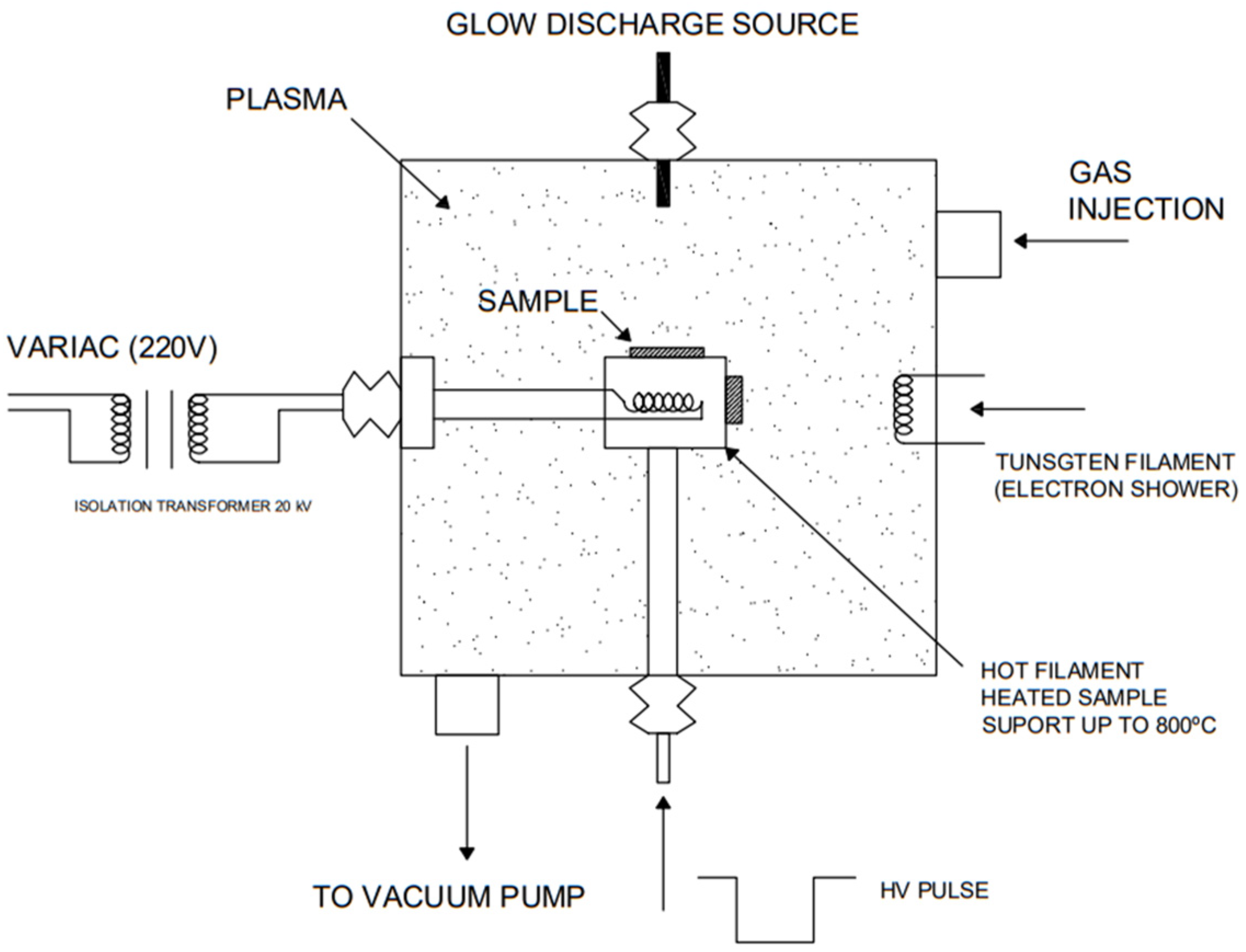
Some samples were subjected to high-energy pulsed-plasma immersion pretreatment in a chamber as shown in Figure 1 prior to their DLC coating to compare their properties with the samples coated only with DLC. The PIII experiments were performed in a UHV system designed and built at IOM in Leipzig, Germany [28,29]. In the references, further information showing a complete schematic drawing of the system is available. The high voltage pulses were supplied by a commercial pulse generator (RUP-4) from GBS Elektronik GmbH (Radeberg, Germany). Nitrogen insertion by PIII was performed in a high-vacuum chamber at a base pressure of 10−5 Pa. At a nitrogen gas flow rate of 150 sccm, the resulting pressure during the experiments was 0.5 Pa. The plasma was generated by an electron cyclotron-resonance (ECR) source operating at a power of 150 W and frequency of 2.54 GHz. Negative high voltage pulses of 10 kV with a rise time of 10 ns/kV and total length of 15 µs were applied to the substrate holder. The process temperature was between 350 and 450 °C for equilibrium pulse frequencies between 0.6 and 1.8 kHz, as determined with a pyrometer calibrated against a thermocouple, over a total process time of 90 min. The incident fluences were around 4.0 × 10¹⁸ nitrogen atoms/cm2.
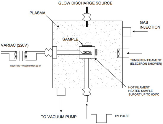
Figure 1.
Scheme of plasma immersion chamber.
2.3. DLC Deposition Technique
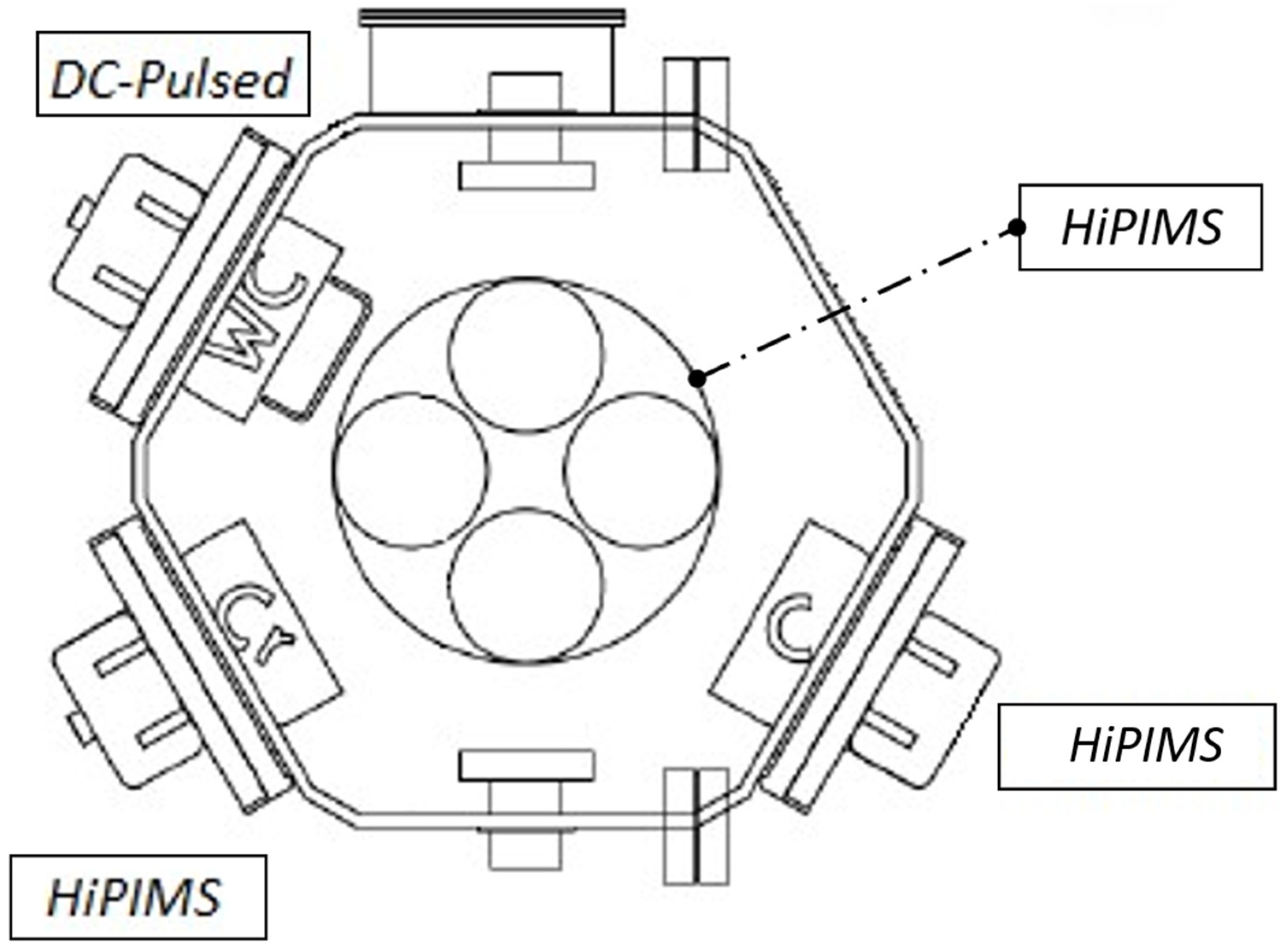
DLC coatings were deposited in an industrial batch-coater designed and manufactured by Nano4Energy SL (Madrid, Spain). The system was integrated into a vacuum chamber of 0.6 m3 with three rectangular cathodes equipped with Cr, WC:Co and C targets. A sketch of the experimental setup is shown in Figure 2.

Figure 2.
Scheme of the HiPIMS chamber in a horizontal cross-section.
The chamber was evacuated by turbomolecular pumps and double-stage rotary vane pumps, reaching a base pressure of 10−6 mbar.
The sequence of parameters used for the different substrate pretreatments, as well as for the deposition of the coatings, is briefly described below following Claver et al. [14].
- Ar etching: An Ar+ discharge was established at the substrates for 15 min, using a direct current (DC)-pulsed bias voltage of −500 V and a frequency of 150 kHz;
- Cr-HiPIMS deposition of a bonding layer: The target was operated in HiPIMS mode with the following parameters: pulsing time of 150 μs, repetition frequency of 300 Hz and an average power density of 5 W/cm2. The substrate voltage bias was adjusted from −750 to −50 V. The deposition rate obtained for a threefold rotation at a substrate voltage bias of −50 V was 0.5 µm/h;
- Deposition of the WC interlayer: WC was deposited in DC-pulsed mode with a power density of 7.5 W/cm2, a frequency rate of 150 kHz and a pulse width of 2.7 µs. The substrate was biased at −50 V. The deposition rate obtained for a threefold rotation was 0.38 µm/h;
- Deposition of the W-doped DLC coating: The power density of the pulses reached values up to 10 W/cm2. The DC-pulsed mode was applied to the carbon target at a repetition frequency of 150 kHz and a pulse width of 2 µs. The HiPIMS mode was applied to the WC:C target with a pulsing time of 150 µs, repetition frequency of 300 Hz, positive pulse of 350 V and power density of 0.5 W/cm2. A substrate voltage bias of −50 V was applied. The deposition rate obtained for a threefold rotation was 0.25 µm/h.
2.4. Thickness, Structural Properties and Profile Composition
Chemical composition profiles were analyzed by glow discharge optical emission spectroscopy (GD-OES) using Jobin Yvon 100000RF equipment (Horiba Instruments, Tokyo, Japan). The phase formation with the PIII was evaluated by means of the ray diffraction using a chromium Kα source (XRD, Bruker, Karlsruhe, Germany) with a wavelength of 0.22897 nm, which is about 50% larger than for Cu Kα. The cross-section images were obtained with a Hitachi S4800 field emission scanning electron microscope (FE-SEM) (Hitachi High-Technologies Corporation, Tokyo, Japan) with a 10.0 kV voltage parameter. The coating thickness was corroborated with CSM Calotest equipment (CSM Instruments, Peseux, Switzerland) using 30 and 25.4 mm diameter stainless-steel balls and superfine diamond water suspension as the abrasive medium.
2.5. Roughness, Mechanical and Tribological Tests
Nanoindentation tests were performed with a Hysitron Triboindenter 950 (Hysitron, Minneapolis, MN, USA) fitted with a Berkovich tip with an end radius of 150 nm. The hardness and the Young’s modulus were obtained according to the method described by Oliver and Pharr [1,2]. Twenty-five indents of 10 mN of maximum load were applied to each sample in order to obtain reliable mean values for both the hardness and the Young’s modulus. The assessment of the adhesion between the substrate and the coating was performed with a CSM Revetest Scratch tester fitted with a Rockwell indenter (diamond cone). The mechanical test was undertaken with a load rate of 100 N/min, a 100 mm/min scratching speed and a final load of 10 mN and a total length of 5 mm; the critical loads of three scratches per sample were averaged.
Different signals were recorded to measure the penetration of the indenter within the substrate, the acoustic emission and the coefficient of friction. Three different critical loads (LCs) were registered:
- The first critical load (LC1): the first cohesive failure registered;
- The second critical load (LC2): the first adhesive failure registered;
- The third critical load (LC3): a total delamination of the coating or a critical defect observed in the reference substrate.
The surface roughness (Sa) of the coated samples was measured by using a confocal S mart microscope (Sensofar, Barcelona, Spain) and following the ISO 25178 standard. A 50× magnification objective was used to measure the Sa values; the current surface length of the measurements was 340.03 µm × 283.73 µm and the following filters were used to obtain the values of the surface roughness (following the ISO 25178):
- Standard cut-off of the high-pass filter: λs = 2.50 µm;
- Standard cut-off of the low-pass filter: λc = 0.08 mm.
Three non-contact 3D areal measurements were carried out in three different zones of each sample.
Microtest equipment in the Pin on Disk configuration was used for the tribomechanical tests. The coefficient of friction (COF) was measured by using a 6 mm alumina ball loaded at 2–5 N, 200 rpm and 6000 and 8000 cycles, respectively. Wear tracks were measured by using a confocal S mart microscope (Sensofar, Barcelona, Spain) and the loss volume as well as the wear evaluation were determined according to the ASTM99 standard.
3. Results
3.1. WC:C Coating by HiPIMS with Positive Pulse
3.1.1. Thickness and Composition
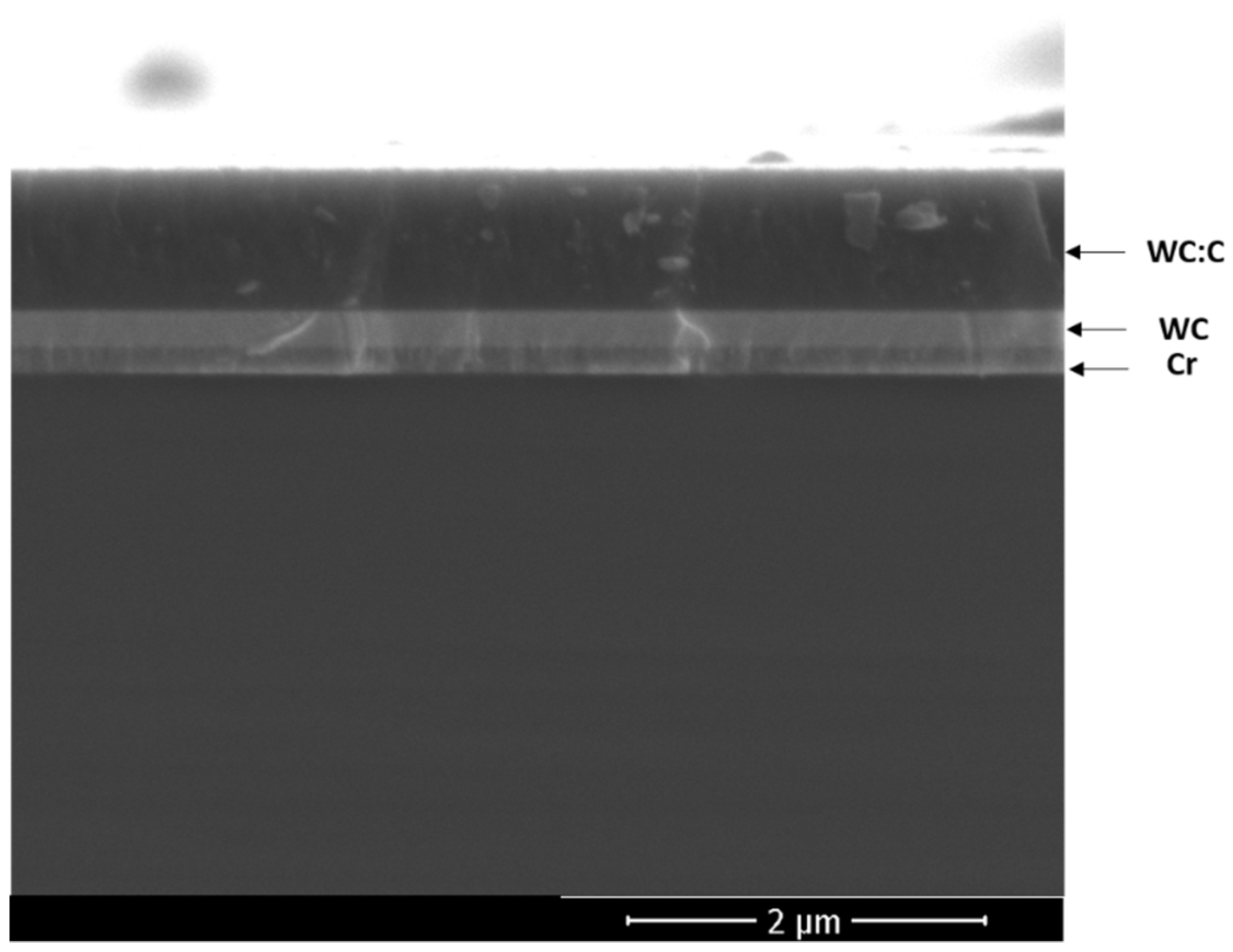
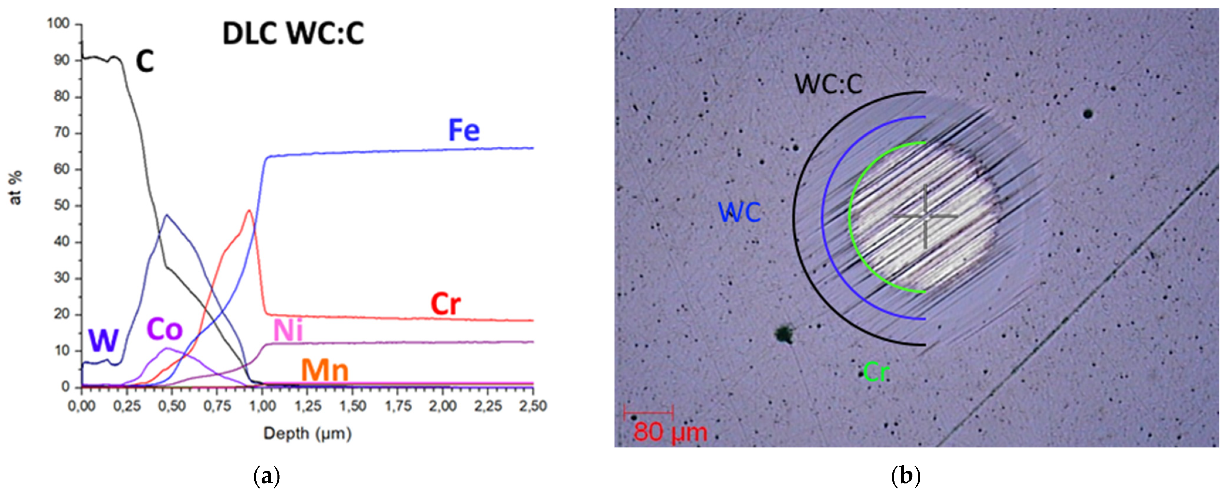
To determine the thickness of the DLC WC:C coating (Figure 3), both a calotest and glow discharge optical emission spectrometry (GDOES) were performed, as shown in Figure 4. The thickness of the thin coating was determined to be around 1 µm for the DLC sample. At that depth, the percentage of chromium reached 45 at.%. This was due to the initial layer of chromium deposited by HiPIMS after the initial Ar etching, which was deposited according to the parameters already established in previous studies [11]. It was used to improve the adherence of the carbon layer.

Figure 3.
Cross-section SEM image with the coating’s structure of DLC WC:C. From bottom to top the image shows the stainless steel substrate, the bonding layer of Cr, the WC interlayer and the W-doped layer.

Figure 4.
(a) Glow discharge optical emission spectrometry (GD-OES) concentration profile of DLC WC:C coating and (b) calotest to determine the coating thickness.
The tungsten content increased to up to 50 at.% when a thickness of 0.5 µm was obtained, at which point it was the same as the carbon. Once this maximum tungsten composition had been reached, the carbon content increased to up to 90% to the detriment of tungsten, which declined to 10% of the total atomic percentage. The composition remained constant at approximately 90%–10% W and C, respectively, in the first 0.2 µm below the surface.
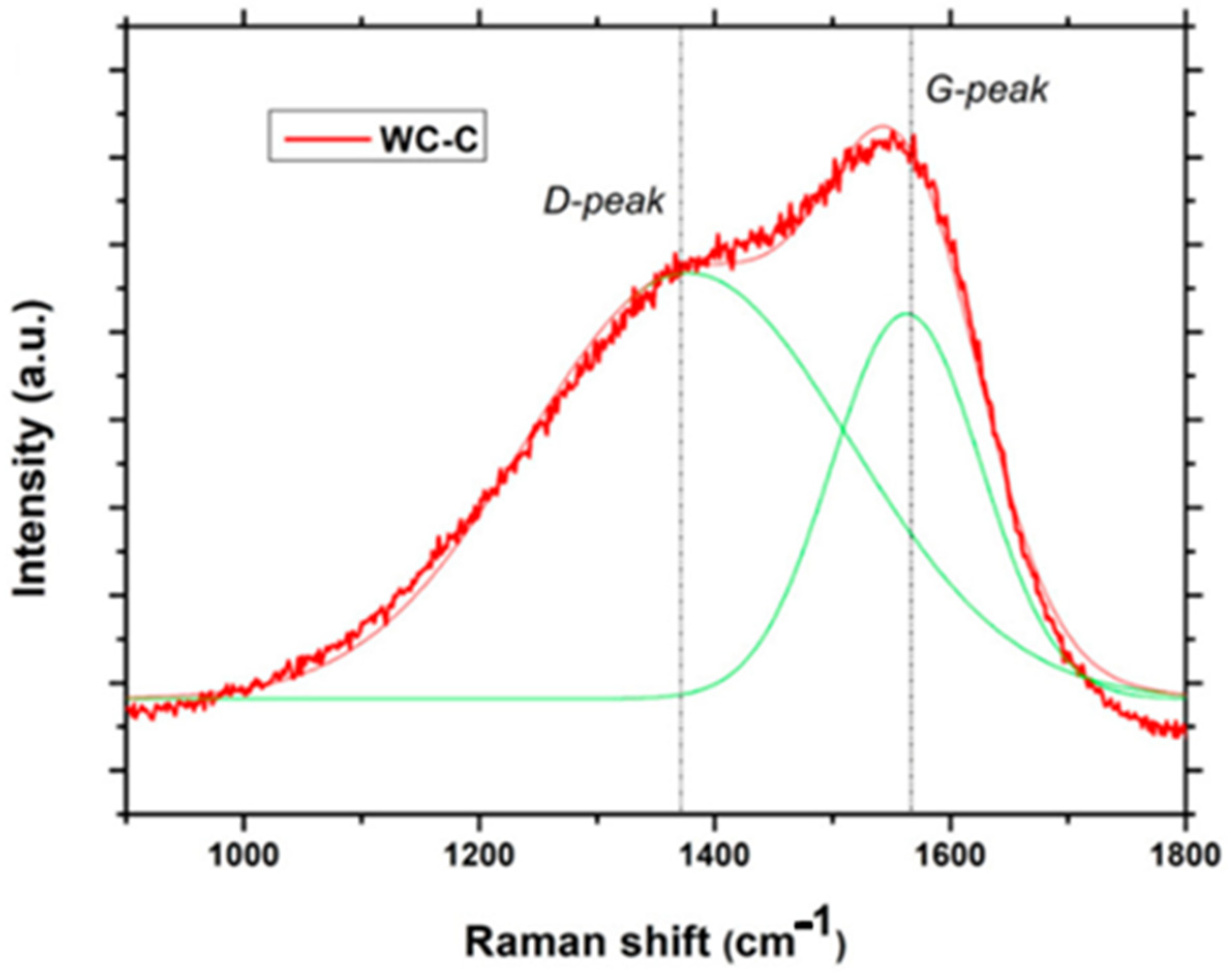
A typical Raman spectrum of the DLC films deposited on the 316L stainless steel is shown in Figure 5. An initial peak is shown which was consistent with the spectrum of aromatic hydrocarbons. In turn, as mentioned above, the concentration of sp3 and the existence of a peak at approximately 1560 cm−1—and therefore aromatic rings—give consistency to the mechanical properties shown by the coatings.
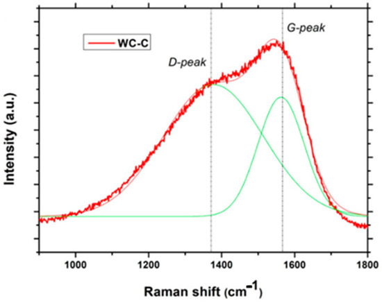
Figure 5.
Raman spectrum of WC:C coating.
The surface roughness after the application of WC: C was Sa = 43.8 ± 7.4 nm. As seen in other studies [30,31], the roughness increased when the DLC coating was deposited, generally due to shading effects during the growth of the film. In addition, the initial roughness of the samples influenced the adhesion of the coating, as previously reported in other investigations [32]. As indicated by Avino et al. [33], the roughness can be reduced by applying a higher positive voltage or by achieving a lower roughness in the initial polishing of the sample.
3.1.2. Nanoindentation Test
The hardness (H), Young’s modulus (E) and H/E and H3/E2 ratios were calculated for both the AISI 316L reference sample and the WC:C coating, as shown in Table 2. The hardness of the substrate was 7.6 GPa, while the WC:C coating showed a hardness of 17.4 GPa. The DLC coating hardness measurements were higher than those obtained using a closed-field unbalanced magnetron sputtering technique, for which values between 11 and 15 GPa were observed [34]. In the load-displacement curves shown in Figure 6, a high elastic component can be observed for WC:C coatings (159–175 GPa), as obtained by Garcia [13].

Table 2.
DLC WC:C nanoindentation results for the hardness (H), Young modulus (E) and their H3/E2 relationship.
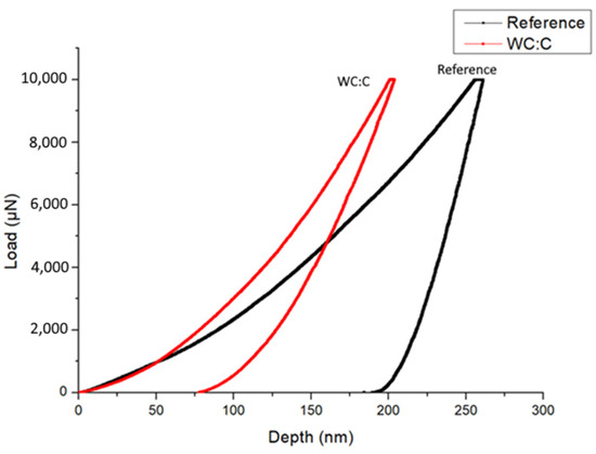
Figure 6.
Nanoindentation curves of the WC:C coating (red line) and reference AISI 316-L (black line) (10 mN).
3.1.3. Adhesion Test
With the aim of determining the adhesion of the coating layer, scratch tests were carried out from 0 to 100 N across a length of 10 mm on the WC:C coating, in which different failure modes were detected along the scratch and evaluated by recording the loads to which they were subjected. The scratch tests showed strongly adhesive behavior. Figure 7 represents the acoustic emission (AE) and the coefficient of friction (COF), i.e., the relationship between the normal and tangential forces as the indenter ploughed the surface.
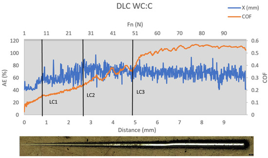
Figure 7.
WC:C coating nano-scratch test: the COF (blue line) and acoustic emission (AE; orange line) evolution vs. the indenter displacement and an optical micrograph of the scratch tracks.
The zones where critical failures appeared and that were detected by the AE signal or a variation in the COF were identified by means of an optical microscope. The loads at which they occurred were recorded (they were show in Table 3) and reached values of 10.5 ± 1.5 N for LC1 (first cohesive failure, Figure 8a), 27.5 ± 1.5 N for LC2 (first trace of adhesive failure and lateral chipping, Figure 8b) and about 48.5 ± 3.5 N for LC3 (more the 50% of the track destroyed and the initiation of lateral cracking, Figure 8c). For LC3, the adhesion reached higher values than the PVD Cr processes reported by Duminica at 35 N or the results from Zhou’s studies with Ti DLC coatings which gave 35.8 N for a 1.82% composition of Ti [35,36]. In the study of low-temperature carburizing DLC coatings undertaken by Boromei for a-C:H, the LC3 was 49 N with a thickness of 3.8 µm [10] (results compared on Table 4).

Table 3.
Experimental data derived from the scratch test with the corresponding values of the critical load (LC1, LC2 and LC3) for the DLC WC:C coating sample.

Figure 8.
Optical images of WC:C-coated sample after nano-scratch test showing (a) LC1, (b) LC2 and (c) LC3.

Table 4.
Experimental data derived from the scratch test for different coatings over a stainless steel substrate [10,35].
3.1.4. Friction and Wear Test
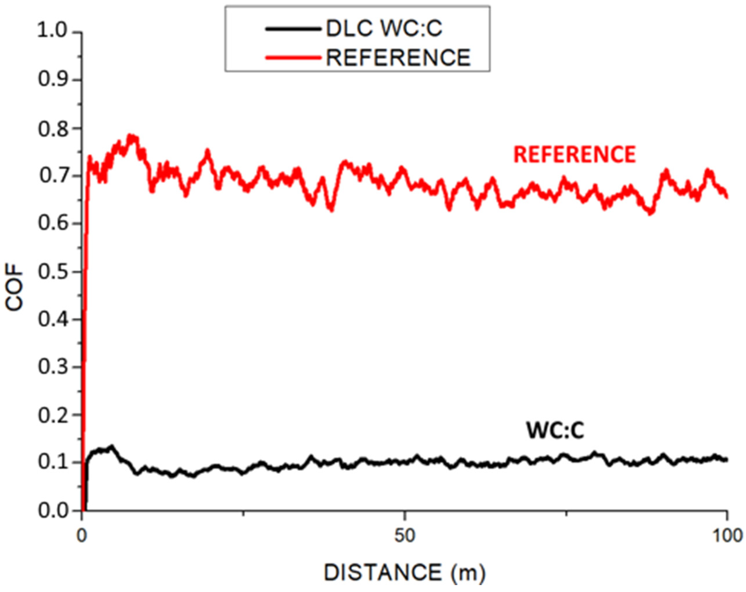
The friction behavior was evaluated by studying friction curves made with a pin-on-disc tribometer with a 6 mm diameter alumina ball. Additionally, the wear tracks were studied to determine the wear properties of the reference sample and the DLC WC:C coating. Coefficient of friction (COF) values of 0.75–0.80 were measured for the reference substrate in the tests carried out at 5 N. The variations were higher in the reference sample because, as the COF and wear rate were higher, this also affects the vibration caused by abrasive phenomena.
The COF for the DLC WC:C coatings at 5 N was measured to be 0.10, as shown in Figure 9. Tungsten oxides can lead to a higher COF before the formation of more lubricious graphitic tribo-layers, as seen in other studies [37]. Here, the COF results were lower than those obtained by Wang et al. [38], where COF values between 0.12–0.37 were reported, or those of Tillman et al. [30], whose results showed COF values between 0.12–0.59 for DLC samples with plasma pretreatment.
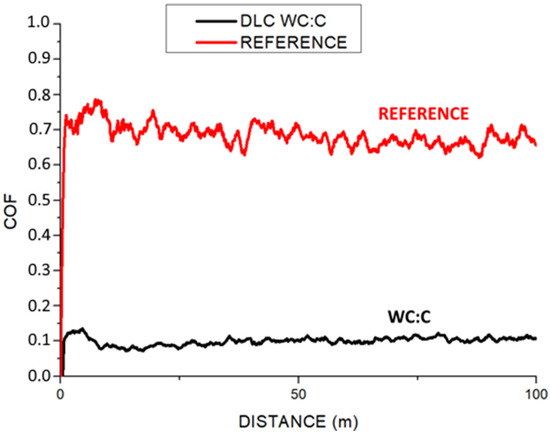
Figure 9.
Friction coefficients of the reference sample and DLC WC:C coating under 5 N.
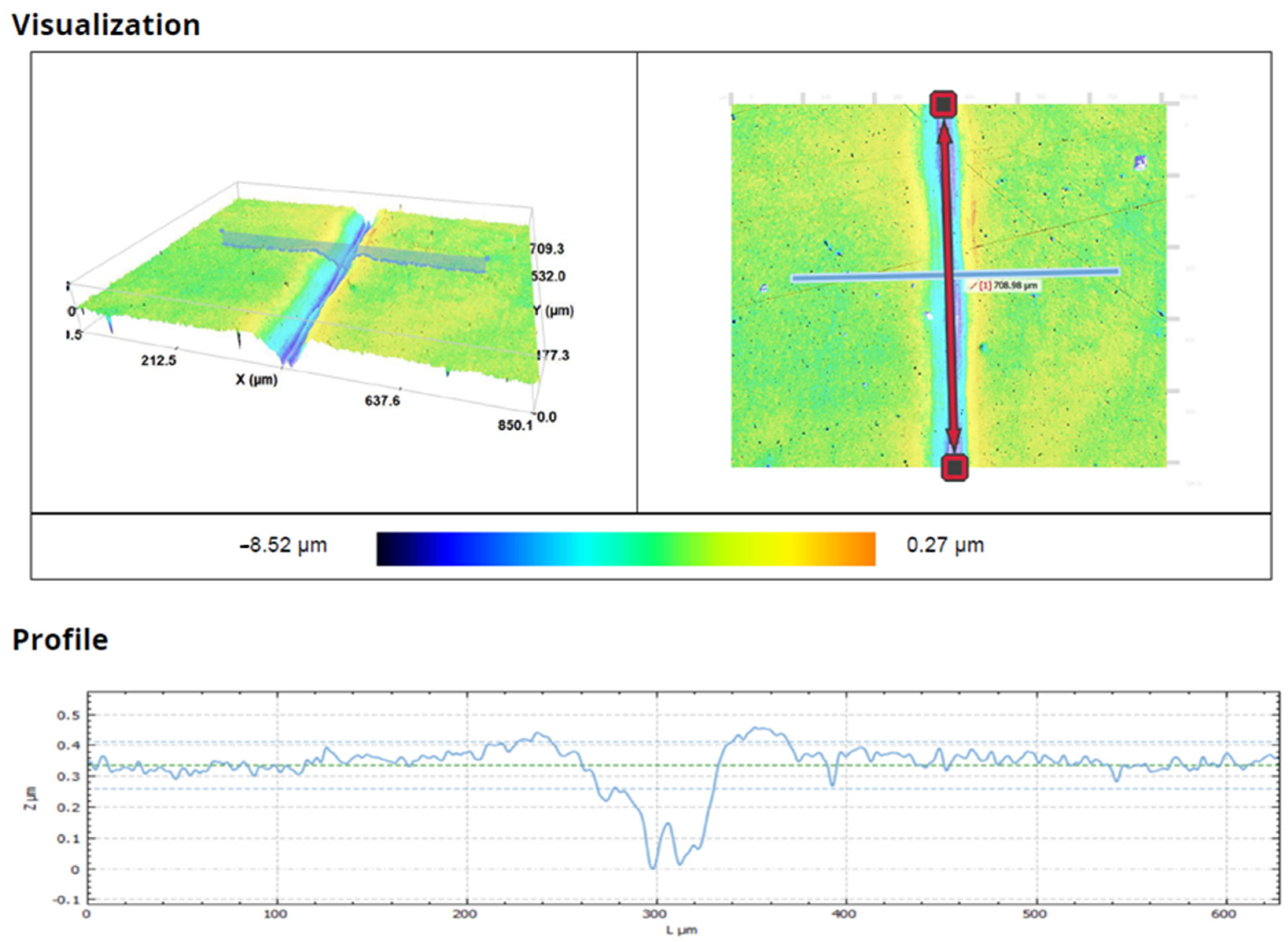
The volume loss in the wear tracks of the reference samples was 3.33 × 10⁻¹⁰ m3. For the DLC coatings, the volume loss (results shown in Table 5 and wear tracks shown in Figure 10) was 4.35 × 10⁻¹³ m3, which implies an important reduction in volume loss of about three orders of magnitude in comparison with the uncoated substrate. The wear coefficient of the reference sample was 6.09 ± 3.75 × 10⁻⁴ mm3/nm and it was 3.96 ± 1.02 × 10⁻⁷ mm3/nm in the DLC WC:C sample.

Table 5.
Summary of the experimental data for the volume loss and wear coefficient measured by confocal microscope for the reference sample and DLC WC:C coating.

Figure 10.
Confocal microscopy after 6000 cycles for the DLC WC:C-coated sample.
3.2. Duplex Samples
3.2.1. Thickness and Composition of Duplex Samples
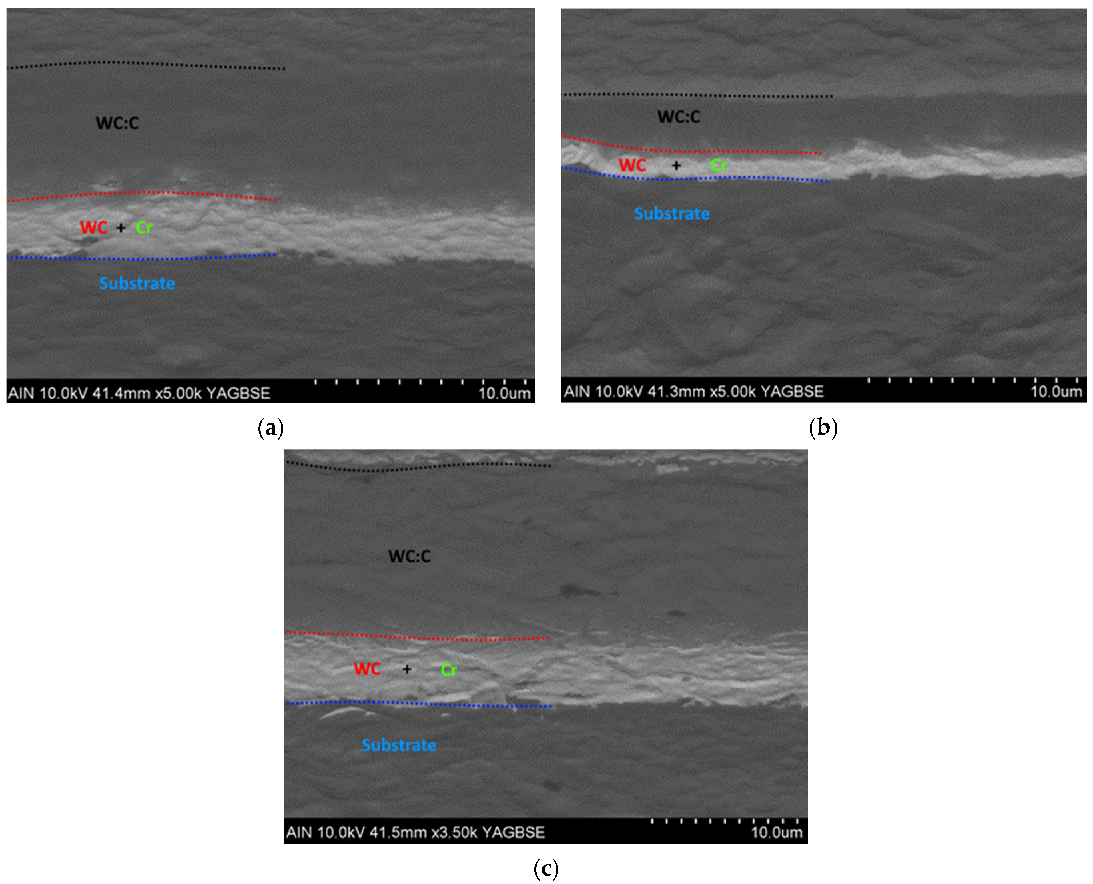
Scanning electron microscope (SEM) images of the cross-sections of the samples were obtained (see Figure 11) using the backscattered electron signal, which provides chemical contrast depending on the elements of the surface (the lighter the image, the heavier the element is).

Figure 11.
SEM cross-section showing the coating structure of (a) PIII + DLC WC:C 350 °C, (b) PIII + DLC WC:C 400 °C and (c) PIII + DLC WC:C 450 °C. From bottom to top, the images show the AISI 316L substrate with the Cr bonding layer, the WC interlayer and the W-doped coat.
The chemical compositions of the DLC coatings were similar for all the samples, as seen in Figure 12. The diffusion of the nitrogen ranged from 1.25 µm for 350 °C through 1.75 µm for 400 °C to more than 3.5 µm for 450 °C.
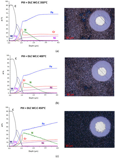
Figure 12.
Glow discharge optical emission spectrometry (GD-OES) concentration profiles and calotests for (a) PIII + DLC WC:C 350 °C, (b) PIII + DLC WC:C 400 °C and (c) PIII + DLC WC:C 450 °C.
The duplex coatings showed different surface roughness values (Table 6): the PIII + WC:C 350 °C sample had Sa = 26.27 ± 2.84 nm, the PIII + WC:C 400 °C sample had Sa = 35.52 ± 2.14 nm and the PIII + WC:C sample 450 °C had Sa = 84.10 ± 13.46 nm, which indicate that with increasing treatment temperature the roughness of the samples increased. The origin of this effect was the increasing ion bombardment during the PIII treatment, as the higher equilibrium temperature necessitated a higher ion current density.

Table 6.
Sa roughness measurements for PIII + WC:C 350 °C, PIII + WC:C 400 °C and PIII + WC:C 450 °C.
Insertion of nitrogen with a concentration of up to 30–35 at.% led to a massive expansion of the austenitic base material, i.e., the formation of expanded austenite characterized by a lattice constant about 5%–12% larger than for the substrate material. The structure, including the grain size, remained intact, with no CrN precipitates, which would have degraded the corrosion resistance, formed at the investigated temperature range of 350–450 °C. The XRD data shown in Figure 13 exemplify this behaviour [31]. The rather low thickness of the modified layer for the 350 °C sample led to the observation of both substrate peaks and of peaks corresponding to the expanded phase (with peaks for (111)-, (200)- and (220)-oriented grains being visible from left to right). For the higher temperatures, the intensity of the substrate peaks was strongly reduced, becoming nearly invisible above the background (due to the thicker layers and the information depth of about 2 µm). No strong variation in the lattice expansion was observed, which was in agreement with the nitrogen surface concentrations shown in Figure 12.
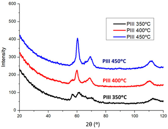
Figure 13.
Chromium Kα-source X-ray diffraction patterns of PIII coatings at 350/400/450 °C.
3.2.2. Nanoindentation Test of Duplex Samples
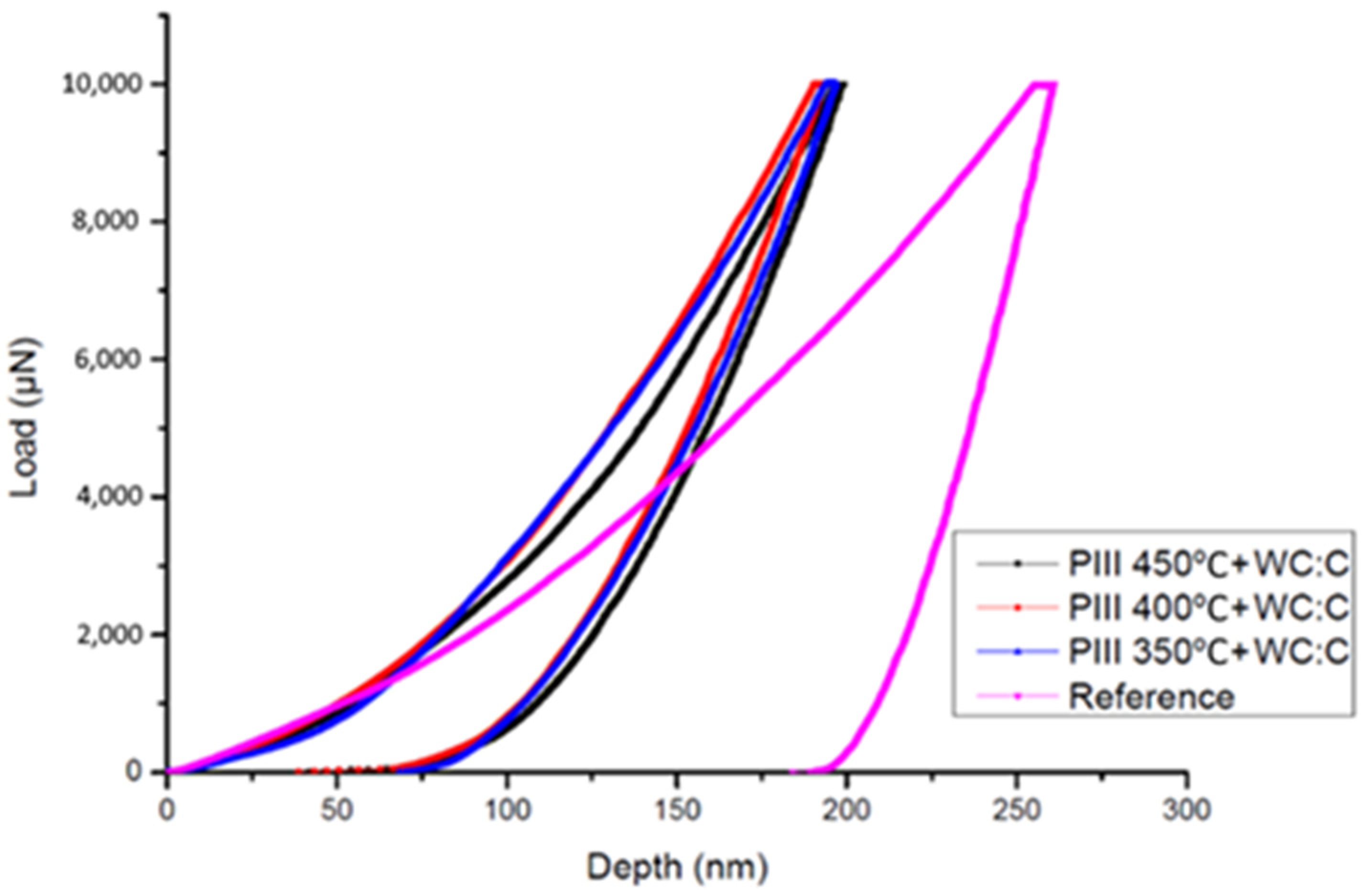
Table 7 shows the hardness (H), Young’s modulus (E) and H/E and H3/E2 ratios for the duplex coatings. The hardness of the substrate was 7.6 GPa. The PIII + DLC WC:C duplex coatings showed hardness values of 16.9, 16.8 and 15.8 GPa for temperatures of 350, 400 and 450 °C, respectively. The hardness of the coating was due to the carbon and tungsten structures that appeared in the surface layers. As seen in the sample with only the DLC coating, there were no great differences observed in the values of the elastic modulus. The resistance to wear and plastic deformation could be increased by increasing the hardness while maintaining the elastic modulus. The load-displacement curves (Figure 14) showed a high elastic component for the three types of duplex coating, without appreciable differences in the temperature variant used in the initial PIII. The results were similar to those obtained for duplex with plasma nitriding plus Ti/TiN multi-layer coatings [39].

Table 7.
Duplex samples’ nanoindentation results for the hardness (H), Young’s modulus (E) and their H/E and H3/E2 relationships.
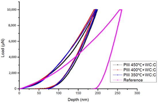
Figure 14.
Nanoindentation curves for the PIII 450 °C + WC:C coating (black line), PIII 400 °C + WC:C coating (red line), PIII 350 °C + WC:C coating (blue line) and reference AISI 316-L (purple line).
3.2.3. Adhesion Test for Duplex Samples
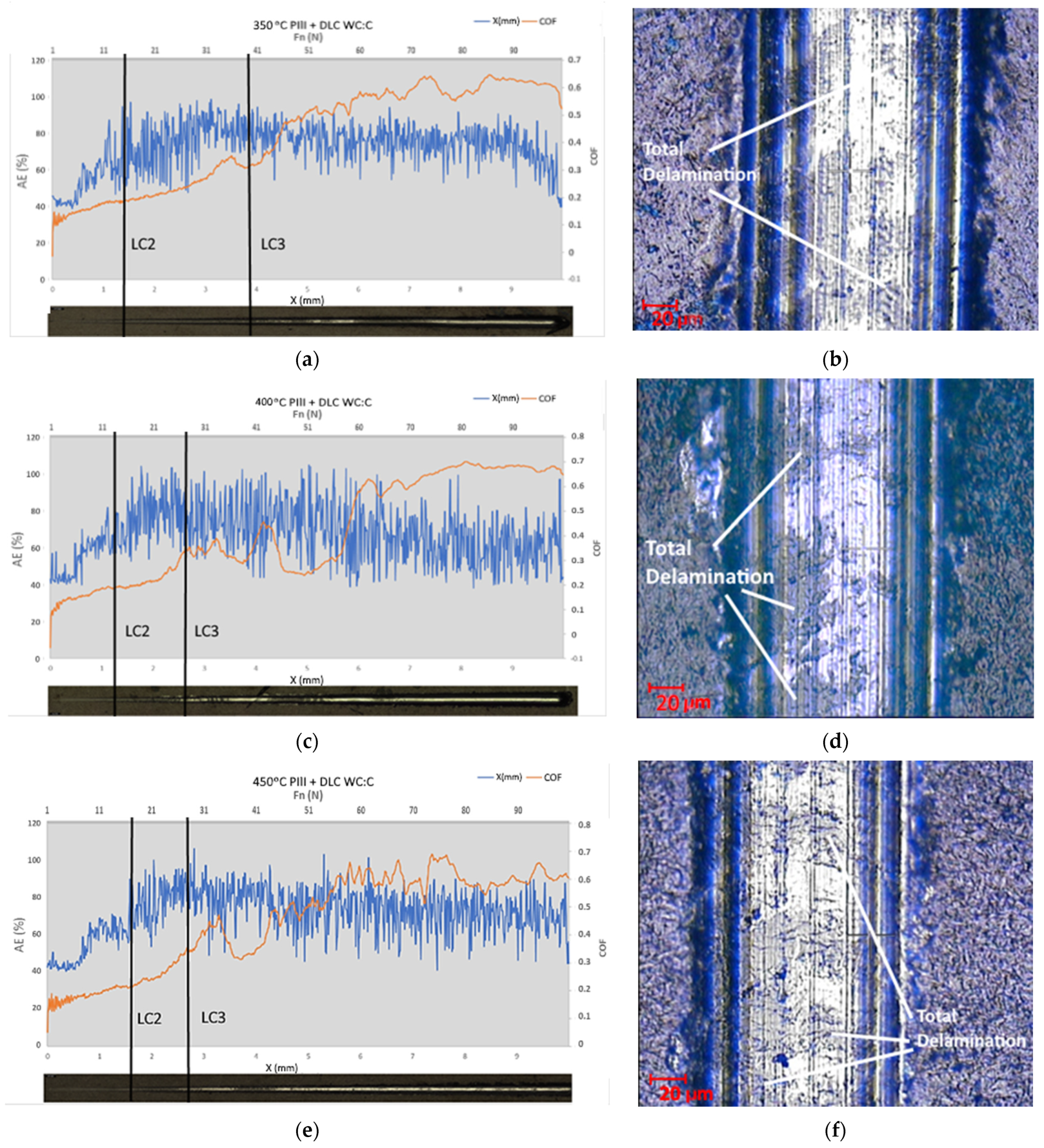
Scratch tests with the same conditions were carried out with the PIII + DLC samples from 0 to 100 N across lengths of 10 mm. The acoustic emission (AE) and coefficient of friction (COF) are shown in Figure 15a,c,e and they were compiled in Table 8. For 350 °C PIII + WC:C, a value of 16.7 N was determined for the LC2 (adhesive failure), which reached up to approximately 38.7 N for the LC3 (removal of the coating with display of the surface in the interior zone of the track, making the substrate visible as in Figure 15b). For 400 °C PIII + WC:C, a value of 13.3 N was determined for the LC2, which reached up to approximately 28.9 N for the LC3 (total delamination with lateral fissuration and removal of the coating, with display of the surface in the interior zone of the track as shown in Figure 15d). For 450 °C PIII + WC:C, a value of 16.7 N was determined for the LC2, which reached up to approximately 28.1 N for the LC3 (continuous full delamination, as shown Figure 15f). Total delamination occurred at lower loads than those studied for the DLC WC:C coatings produced using HiPIMS with positive pulses. The results obtained were higher than those obtained with other techniques for samples with a hardness of 316L hardness [40] but lower than the results shown above for the DLC coating. This may have been due to the appearance of a layer of oxynitrides induced by insufficient initial surface cleaning during the Ar etching, which would have decreased the adhesion of the coating. The first cohesive failure (LC1) was not detected due to surface inhomogeneities, which made it impossible to detect the typical cohesive failure cracks in the center of the scratch track.

Figure 15.
Scratch test of (a) 350 °C PIII + DLC WC:C and (b) the critical load LC3, (c) 400 °C PIII + DLC WC:C with (d) the LC3 and (e) 450 °C PIII + DLC WC:C with (f) the LC3. COF (blue line) and acoustic emission (AE; orange line) evolution vs. indenter displacements and optical micrographs of the scratch tracks.

Table 8.
Experimental data derived from the scratch tests with the corresponding values of the critical loads (LC1, LC2 and LC3) for the DLC WC:C coating sample.
3.2.4. Friction and Wear Test of Duplex Samples
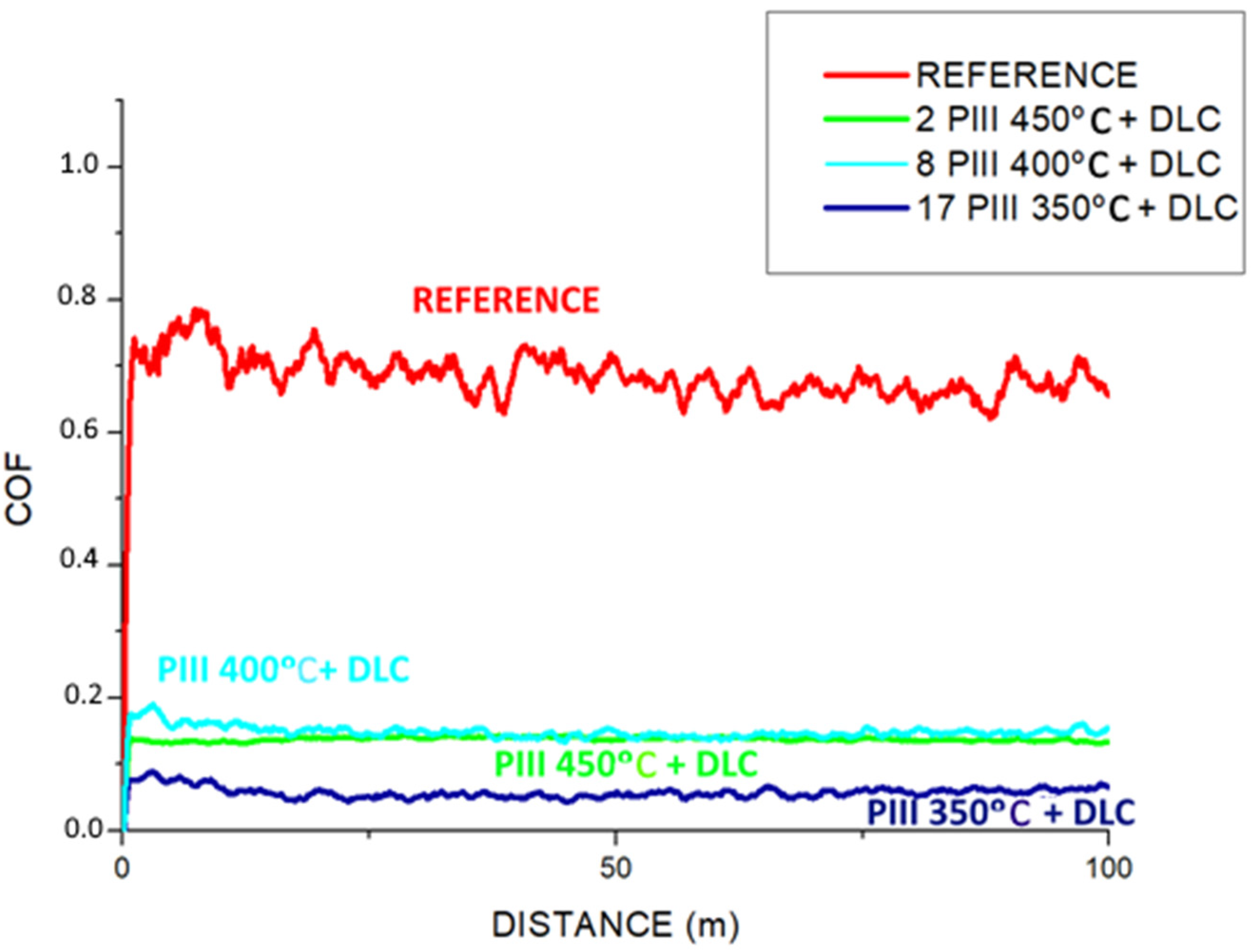
The coefficient of friction (COF) for the 350 °C PIII + WC:C sample was 0.08, whereas for the 400 °C PIII + WC:C and 450 °C samples it was 0.15 (COF results shown in Figure 16). The COF results were lower than those reported by Laura et al., Boromei or Fuentes et al. [10,41,42], where coatings of plasma nitriding and TiTiN or LTC/a-C:H were both measured to have values larger than 0.6 and a CrCN PVD was measured at 0.2. For a DLC with plasma pretreatment, COF values between 0.12 and 0.59 were obtained in the study by Tillman et al. [30].
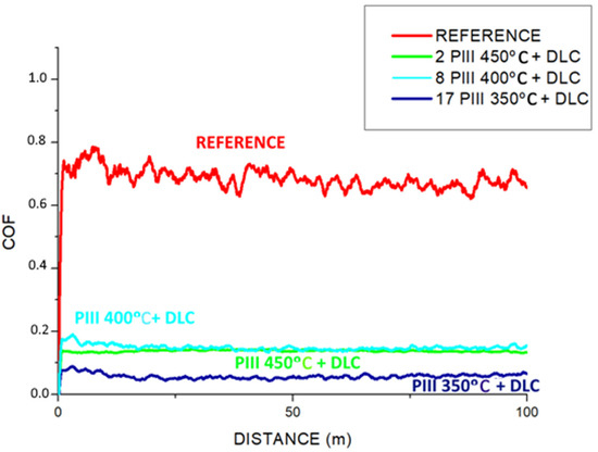
Figure 16.
Friction coefficients of the PIII 450 °C + WC:C coating (red line), PIII 400 °C + WC:C coating (blue line), PIII 350 °C + WC:C coating (purple line) and the reference AISI 316-L (green line) under 5 N.
The data for the volume loss in the wear tracks are shown in Table 9. The base material 316L was taken as a reference with a loss of 3.33 × 10⁻¹⁰ m3. For 350 °C PIII + WC:C, the volume loss was reported to be 1.04 × 10⁻¹² m3; for 400 °C PIII + WC:C, it was 7.76 × 10⁻¹³ m3; and for 450 °C PIII + WC:C, it was 6.05 × 10⁻¹³ m3, which implied a loss of volume similar to that reported for the single-layer coating of DLC. Regarding the wear coefficient, measurements were made for the three samples. For 350 °C PIII + WC:C, the wear coefficient was found to be 4.09 × 10⁻⁷ mm3/nm; for 400 °C PIII + WC:C, it was 3.18 × 10⁻⁷ mm3/nm; and for 450 °C PIII + WC:C, it was 2.57 × 10⁻⁷ mm3/nm, which represent wear coefficients within the range of values obtained for the DLC coating.

Table 9.
Summary of the experimental data for the volume loss and wear coefficient measured by confocal microscope for the reference and DLC WC:C coating.
4. Discussion
The HiPIMS technique with positive pulses increased the adhesion of DLC coatings on stainless steel samples, reaching LC2 and LC3 values of around 28 and 49 N, respectively. However, the PIII + DLC duplex technique obtained lower values than the DLC coating, with LC2 and LC3 values of 13–17 and 28–39 N depending on the applied PIII temperatures, which reduced the adherence of the coating to the substrate obtained by HiPIMS with positive pulses.
However, the duplex coating showed similar adhesion properties to other techniques studied with thicker coatings [9,43]. It could be suggested that the initial cleaning for the removal of surface oxides could have caused the appearance of oxynitrides between both coatings, producing a failure point for the metal–metal adhesion sought for the DLC on the nitride substrate. Native oxides and hydroxides promote weak metal–oxide bonding in comparison with metal–metal bonding, which decreases the interface strength. These negative effects are particularly evident when DLC is deposited onto steel substrates, and for this reason a number of techniques have been developed as pretreatment steps to improve DLC adhesion [4].
As confirmed by Schoeppner et al. [44], scratch tests can be used in future studies as a method of determining the intrinsic stress and the applied stress necessary to delaminate a coating.
To improve the adhesion, it is suggested to use a treatment in an isolated system, which helps to avoid contamination and reduce the nitrogen profile, thus optimizing the surface finish prior to the deposition of the DLC.
The use of W-doped DLC (WC:C) coatings was not primarily for the purpose of achieving hard coatings. The W tends to destabilize the sp3 phase of the carbon and thus reduce the hardness. Typically, metal-doped DLC coatings are used because they make it possible to obtain a DLC with reduced stress and greater load support for tribological applications involving subjection to high loads and requiring low friction [45]. By adjusting the concentrations of metals such as W, Ti and Cr in the carbon matrix, it should be possible to form carbide nanoclusters that restrict deformation and crack propagation.
The wear data showed that the application of the DLC coating improved the wear resistance. Wear resistance was also improved as a function of PIII processing temperature. By increasing the treatment temperature, the nitrogen profile increased, as well as its depth, which facilitated the desired duplex effect and thus also the resistance to wear. A more in-depth study is needed to determine the influences of these parameters and clarify whether this wear resistance increase is dependent on the treatment temperature.
5. Conclusions
In this work, the application of DLC coatings through HiPIMS with positive pulses onto stainless steel samples was studied. The adhesion properties and resistance to wear were studied and the friction coefficient determined, and the following conclusions were reached:
- The nanohardness of the DLC WC:C was in the range of 18 GPa, which is typical of this kind of coating;
- The nanohardness for the duplex samples was between 14.5 and 19.8 GPa, as often seen in this type of coating;
- The adherence of the DLC WC:C obtained through HIPIMS with positive pulses presented a maximum critical load (LC3) of 52 N, higher than the results shown in previous studies on DLCs deposited on stainless steels;
- Simple and duplex DLC coatings were found to exhibit a significant increase in wear resistance compared to uncoated samples;
- The HiPIMS with positive pulses made it possible to increase the critical load, which was indicative of an improvement in adhesion and led to an improvement in the wear resistance of the DLC coatings;
- PIII pretreatments did not increase the coating adhesion but slightly increased the wear resistance.
Further studies are necessary to determine the cause of this improvement in wear behavior and to determine the cause of the loss of adhesion in the duplex samples.
Author Contributions
Conceptualization, I.G., J.A.G. and A.C.; formal analysis, J.A.G., I.G. and A.C.; investigation, I.G., J.A.G., A.C., S.M., C.D., I.F., J.F.P. and J.A.S.; resources, I.G.; writing—original draft preparation, I.G. and J.A.G.; writing—review and editing, I.G., A.C., J.A.G., J.F.P., C.D., S.M. and J.A.S.; supervision, J.A.G.; project administration, I.G. and J.A.G.; funding acquisition, I.G. and J.A.G. All authors have read and agreed to the published version of the manuscript.
Funding
This research was supported by Government of Navarra grants for the hiring of doctoral students by companies and research and knowledge dissemination organizations: industrial doctorates 2019–2021, grant number 0011-1408-2018-000000.
Institutional Review Board Statement
Not applicable.
Informed Consent Statement
Not applicable.
Data Availability Statement
Data is contained within the article.
Acknowledgments
Thanks to Joycar and Seinsa Corporation for the support provided to the authors and the research. AIN acknowledges the support of CDTI Ministerio de Ciencia e Innovación of Spain through the project CERVERA (CER2019-1003).
Conflicts of Interest
The authors declare no conflict of interest.
References
- Bewilogua, K.; Hofmann, D. History of diamond-like carbon films—From first experiments to worldwide applications. Surf. Coat. Technol. 2014, 242, 214–225. [Google Scholar] [CrossRef]
- Moura e Silva, C.W.; Alves, E.; Ramos, A.R.; Sandu, C.S.; Cavaleiro, A. Adhesion failures on hard coatings induced by interface anomalies. Vacuum 2009, 83, 1213–1217. [Google Scholar] [CrossRef]
- Lin, J.; Sproul, W.D.; Wei, R.; Chistyakov, R. Diamond like carbon films deposited by HiPIMS using oscillatory voltage pulses. Surf. Coat. Technol. 2014, 258, 1212–1222. [Google Scholar] [CrossRef]
- Santiago, J.A.; Fernández-Martínez, I.; Wennberg, A.; Molina-Aldareguia, J.M.; Castillo-Rodríguez, M.; Rojas, T.C.; Sánchez-López, J.C.; González, M.U.; García-Martín, J.M.; Li, H.; et al. Adhesion enhancement of DLC hard coatings by HiPIMS metal ion etching pretreatment. Surf. Coat. Technol. 2018, 349, 787–796. [Google Scholar] [CrossRef]
- Santiago, J.A.; Fernández-Martínez, I.; Sánchez-López, J.C.; Rojas, T.C.; Wennberg, A.; Bellido-González, V.; Molina-Aldareguia, J.M.; Monclús, M.A.; González-Arrabal, R. Tribomechanical properties of hard Cr-doped DLC coatings deposited by low-frequency HiPIMS. Surf. Coat. Technol. 2020, 382, 124899. [Google Scholar] [CrossRef]
- Shukla, K.; Sugumaran, A.A.; Khan, I.; Ehiasarian, A.P.; Hovsepian, P.E. Low pressure plasma nitrided CoCrMo alloy utilising HIPIMS discharge for biomedical applications. J. Mech. Behav. Biomed. Mater. 2020, 111, 104004. [Google Scholar] [CrossRef]
- Sharma, N.; Kumar, N.; Dash, S.; Das, C.R.; Subba Rao, R.V.; Tyagi, A.K.; Raj, B. Scratch resistance and tribological properties of DLC coatings under dry and lubrication conditions. Tribol. Int. 2012, 56, 129–140. [Google Scholar] [CrossRef]
- Fu, T.; Zhou, Z.F.; Zhou, Y.M.; Zhu, X.D.; Zeng, Q.F.; Wang, C.P.; Li, K.Y.; Lu, J. Mechanical properties of DLC coating sputter deposited on surface nanocrystallized 304 stainless steel. Surf. Coat. Technol. 2012, 207, 555–564. [Google Scholar] [CrossRef]
- Dalibón, E.L.; Heim, D.; Forsich, C.; Rosenkranz, A.; Guitar, M.A.; Brühl, S.P. Characterization of thick and soft DLC coatings deposited on plasma nitrided austenitic stainless steel. Diam. Relat. Mater. 2015, 59, 73–79. [Google Scholar] [CrossRef]
- Boromei, I.; Ceschini, L.; Marconi, A.; Martini, C. A duplex treatment to improve the sliding behavior of AISI 316L: Low-temperature carburizing with a DLC (a-C:H) topcoat. Wear 2013, 302, 899–908. [Google Scholar] [CrossRef]
- Dong, H.; He, Z.; Zhang, S.; Sun, D. Effect of temperature and bias voltage on electrical and electrochemical properties of diamond-like carbon films deposited with HiPIMS. Surf. Coat. Technol. 2019, 358, 987–993. [Google Scholar] [CrossRef]
- Morshed, M.M.; McNamara, B.P.; Cameron, D.C.; Hashmi, M.S.J. Stress and adhesion in DLC coatings on 316L stainless steel deposited by a neutral beam source. J. Mater. Process. Technol. 2003, 141, 127–131. [Google Scholar] [CrossRef]
- García, J.A.; Rivero, P.J.; Barba, E.; Fernández, I.; Santiago, J.A.; Palacio, J.F.; Fuente, G.G.; Rodríguez, R.J. A comparative study in the tribological behavior of DLC coatings deposited by HiPIMS technology with positive pulses. Metals 2020, 10, 174. [Google Scholar] [CrossRef] [Green Version]
- Claver, A.; Jiménez-Piqué, E.; Palacio, J.F.; Almandoz, E.; De Ara, J.F.; Fernández, I.; Santiago, J.A.; Barba, E.; García, J.A. Comparative study of tribomechanical properties of HiPIMS with positive pulses DLC coatings on different tools steels. Coatings 2021, 11, 28. [Google Scholar] [CrossRef]
- Santiago, J.A.; Fernández-Martínez, I.; Kozák, T.; Capek, J.; Wennberg, A.; Molina-Aldareguia, J.M.; Bellido-González, V.; González-Arrabal, R.; Monclús, M.A. The influence of positive pulses on HiPIMS deposition of hard DLC coatings. Surf. Coat. Technol. 2019, 358, 43–49. [Google Scholar] [CrossRef]
- Sha, C.; Zhou, Z.; Xie, Z.; Munroe, P. Scratch response and tribological behaviour of CrAlNiN coatings deposited by closed field unbalanced magnetron sputtering system. Surf. Coat. Technol. 2019, 367, 30–40. [Google Scholar] [CrossRef]
- Kabir, M.S.; Munroe, P.; Zhou, Z.; Xie, Z. Scratch adhesion and tribological behaviour of graded Cr/CrN/CrTiN coatings synthesized by closed-field unbalanced magnetron sputtering. Wear 2017, 380–381, 163–175. [Google Scholar] [CrossRef]
- Warcholinski, B.; Gilewicz, A.; Myslinski, P.; Dobruchowska, E.; Murzynski, D. Structure and properties of AlCrN coatings deposited using cathodic arc evaporation. Coatings 2020, 10, 793. [Google Scholar] [CrossRef]
- Kumar, C.S.; Patel, S.K. Performance analysis and comparative assessment of nano-composite TiAlSiN/TiSiN/TiAlN coating in hard turning of AISI 52100 steel. Surf. Coat. Technol. 2018, 335, 265–279. [Google Scholar] [CrossRef]
- Drábik, M.; Truchlý, M.; Ballo, V.; Roch, T.; Kvetková, L.; Kúš, P. Influence of substrate material and its plasma pretreatment on adhesion and properties of WC/a-C:H nanocomposite coatings deposited at low temperature. Surf. Coat. Technol. 2018, 333, 138–147. [Google Scholar] [CrossRef]
- dos Santos de Almeida, E.A.; Milan, J.C.G.; da Costa, C.E.; Binder, C.; de Mello, J.D.B.; Costa, H.L. Combined use of surface texturing, plasma nitriding and DLC coating on tool steel. Coatings 2021, 11, 201. [Google Scholar] [CrossRef]
- Kessler, O.; Surm, H.; Hoffmann, F.; Mayr, P. Enhancing surface hardness of titanium alloy Ti-6Al-4V by combined nitriding and CVD coating. Surf. Eng. 2002, 18, 299–304. [Google Scholar] [CrossRef]
- Tan, C.; Zhou, K.; Kuang, T.; Li, Y.; Ma, W. Novel performances of in situ plasma nitriding-PVD duplex-treated nanocrystalline TiN coatings. Surf. Eng. 2018, 34, 520–526. [Google Scholar] [CrossRef]
- Mändl, S.; Günzel, R.; Richter, E.; Möller, W. Nitriding of austenitic stainless steels using plasma immersion ion implantation. Surf. Coat. Technol. 1998, 100–101, 372–376. [Google Scholar] [CrossRef]
- Mändl, S.; Dunkel, R.; Hirsch, D.; Manova, D. Intermediate stages of CrN precipitation during PIII nitriding of austenitic stainless steel. Surf. Coat. Technol. 2014, 258, 722–726. [Google Scholar] [CrossRef]
- Schibicheski Kurelo, B.C.E.; de Souza, G.B.; Serbena, F.C.; de Oliveira, W.R.; Marino, C.E.B.; Taminato, L.A. Performance of nitrogen ion-implanted supermartensitic stainless steel in chlorine- and hydrogen-rich environments. Surf. Coat. Technol. 2018, 351, 29–41. [Google Scholar] [CrossRef]
- Medrano, A.; Rico, M.; Sanchez, R.; Martínez, R.; García, J.A. Niche sectors for economically competitive ion implantation treatments. Surf. Coat. Technol. 2002, 159, 48–53. [Google Scholar]
- Mändl, S.; Manova, D. Modification of metals by plasma immersion ion implantation. Surf. Coat. Technol. 2019, 365, 83–93. [Google Scholar] [CrossRef]
- Mändl, S.; Lutz, J.; Díaz, C.; Gerlach, J.W.; García, J.A. Reprint of “Influence of reduced current density on diffusion and phase formation during PIII nitriding of austenitic stainless steel and CoCr alloys”. Surf. Coat. Technol. 2014, 256, 78–84. [Google Scholar] [CrossRef]
- Tillmann, W.; Lopes Dias, N.F.; Stangier, D. Influence of plasma nitriding pretreatments on the tribo-mechanical properties of DLC coatings sputtered on AISI H11. Surf. Coat. Technol. 2019, 357, 1027–1036. [Google Scholar] [CrossRef]
- Lin, J.; Zhang, X.; Ge, F.; Huang, F. Thick CrN/AlN superlattice coatings deposited by hot filament assisted HiPIMS for solid particle erosion and high temperature wear resistance. Surf. Coat. Technol. 2019, 377, 124922. [Google Scholar] [CrossRef]
- Takadoum, J.; Houmid Bennani, H. Influence of substrate roughness and coating thickness on adhesion, friction and wear of TiN films. Surf. Coat. Technol. 1997, 96, 272–282. [Google Scholar] [CrossRef]
- Avino, F.; Fonnesu, D.; Koettig, T.; Bonura, M.; Senatore, C.; Perez Fontenla, A.T.; Sublet, A.; Taborelli, M. Improved film density for coatings at grazing angle of incidence in high power impulse magnetron sputtering with positive pulse. Thin Solid Film. 2020, 706, 138058. [Google Scholar] [CrossRef]
- Pu, J.; He, D.; Wang, L. Effects of WC phase contents on the microstructure, mechanical properties and tribological behaviors of WC/a-C superlattice coatings. Appl. Surf. Sci. 2015, 357, 2039–2047. [Google Scholar] [CrossRef]
- Zhou, Y.; Li, L.; Shao, W.; Chen, Z.; Wang, S.; Xing, X.; Yang, Q. Mechanical and tribological behaviors of Ti-DLC films deposited on 304 stainless steel: Exploration with Ti doping from micro to macro. Diam. Relat. Mater. 2020, 107, 107870. [Google Scholar] [CrossRef]
- Duminica, F.D.; Belchi, R.; Libralesso, L.; Mercier, D. Investigation of Cr(N)/DLC multilayer coatings elaborated by PVD for high wear resistance and low friction applications. Surf. Coat. Technol. 2018, 337, 396–403. [Google Scholar] [CrossRef]
- Voevodin, A.A.; O’Neill, J.P.; Zabinski, J.S. Tribological performance and tribochemistry of nanocrystalline WC/amorphous diamond-like carbon composites. Thin Solid Film. 1999, 342, 194–200. [Google Scholar] [CrossRef]
- Wang, L.; Li, L.; Kuang, X. Effect of substrate bias on microstructure and mechanical properties of WC-DLC coatings deposited by HiPIMS. Surf. Coat. Technol. 2018, 352, 33–41. [Google Scholar] [CrossRef]
- Samanta, A.; Rane, R.; Kundu, B.; Chanda, D.K.; Ghosh, J.; Bysakh, S.; Jhala, G.; Joseph, A.; Mukherjee, S.; Das, M.; et al. Bio-tribological response of duplex surface engineered SS316L for hip-implant application. Appl. Surf. Sci. 2020, 507, 145009. [Google Scholar] [CrossRef]
- Grenadyorov, A.S.; Solovyev, A.A.; Oskomov, K.V. The effect of duplex processing on the mechanical properties of grade 316L stainless steel. Tech. Phys. Lett. 2020, 46, 1060–1063. [Google Scholar] [CrossRef]
- Vaca, L.S.; Quintana, J.P.; Vega, D.; Márquez, A.; Brühl, S.P. Tribological and corrosion behavior of duplex coated AISI 316L using plasma based ion implantation and deposItion. Mater. Today Commun. 2020, 26, 101892. [Google Scholar] [CrossRef]
- Fuentes, G.G.; Díaz de Cerio, M.J.; García, J.A.; Martínez, R.; Bueno, R.; Rodríguez, R.J.; Rico, M.; Montalá, F.; Qin, Y. Gradient CrCN cathodic arc PVD coatings. Thin Solid Film. 2009, 517, 5894–5899. [Google Scholar] [CrossRef]
- Grenadyorov, A.S.; Oskirko, V.O.; Solovyev, A.A.; Oskomov, K.V.; Khlusov, I.A. Wear and corrosion resistance of a-C:H:SiOx coating on medical 316L stainless steel. J. Mater. Eng. Perform. 2021, 30, 1099–1109. [Google Scholar] [CrossRef]
- Schoeppner, R.L.; Putz, B.; Taylor, A.A.; Pethö, L.; Thomas, K.; Antonin, O.; Nelis, T.; Michler, J. Combinatorial materials design approach to investigate adhesion layer chemistry for optimal interfacial adhesion strength. Crystals 2021, 11, 357. [Google Scholar] [CrossRef]
- Fontaine, J.; Donnet, C.; Erdemir, A. Fundamentals of the Tribology of DLC Coatings; Springer: Boston, MA, USA, 2008; ISBN 9780387302645. [Google Scholar]
Publisher’s Note: MDPI stays neutral with regard to jurisdictional claims in published maps and institutional affiliations. |
© 2021 by the authors. Licensee MDPI, Basel, Switzerland. This article is an open access article distributed under the terms and conditions of the Creative Commons Attribution (CC BY) license (https://creativecommons.org/licenses/by/4.0/).

