1. Introduction
Power management, i.e., the conditioning and control of electrical energy, is a critical function in many electronic systems. Generators and batteries deliver voltages and currents that exhibit variations over time and across a broad spectrum of operation conditions. A voltage regulator is employed to convert this fluctuating voltage into a stable, constant, precise, and load-independent output [
1]. Traditional low-dropout regulators (LDOs) with large external output capacitors have been preferred for their superior load transient response; however, these configurations consume more area and are not suitable for system-on-chip (SoC) applications. Therefore, output-capacitor-less LDOs (OCL-LDOs) have emerged as the preferred architectures, aligning with the pursuit of efficiency and compactness [
2,
3,
4,
5,
6,
7].
The design of an OCL-LDO entails a careful balance of multiple performance metrics. One primary specification is the minimization of the quiescent current
, as it directly impacts the battery longevity in IoT devices, many of which predominantly operate in ultra-low power or standby modes [
8]. From the dynamic performance perspective, it is essential to achieve a high control loop bandwidth (BW) and a high slew rate (SR), factors that directly influence the gate driving capability of the pass transistor and, consequently, transient response characteristics [
9,
10,
11]. However, enhancing these parameters frequently results in increased power consumption, highlighting an intricate trade-off in LDO design. Beyond these metrics, design considerations extend to improving the load transient response, reducing the settling/recovery time, and increasing the power supply rejection ratio (PSRR), ensuring the OCL-LDO addresses contemporary electronic demands without compromising on power efficiency.
The classic CMOS LDO regulator topology is shown in
Figure 1. It consists of an error amplifier (EA), a PMOS pass transistor located between the unregulated input
and the regulated output
, and a resistive negative feedback network
–
. The EA compares the reference voltage
and the proportionally scaled output voltage, sensed through
–
and defined as
. In response to these voltage variations, the EA modulates the gate of the PMOS pass transistor, ensuring the precise current delivery to the load (represented by
,
), across the entire operational
domain. Regulation ensures the stability of the output voltage
, which is given assuming an ideal EA, by:
One of the inherent challenges when designing an OCL-LDO is that the dominant pole is typically associated with the gate of the pass transistor, complicating the compensation process since as the output pole is load dependent, the relative position of the poles becomes load-dependent [
6]. To address this issue, different compensation techniques have been introduced over the years. Noteworthy strategies include nested Miller compensation [
12], reverse nested Miller compensation [
13], and pole-zero cancellation, being the case where
= 0 (no-load), the most critical in terms of stability [
14].
On the other hand, adaptive biasing and dynamic biasing are strategies commonly used to enhance the dynamic performance of the LDO regulator. In [
15], adaptive biasing is combined with two cross-summed transconductance cells to achieve a quiescent current
as low as 25 nA and voltage peaks
below 275 mV. However, under maximum load conditions,
reaches up to 45 μA. In general, this technique enhances the dynamic response by extending the gain–bandwidth product (GBW) under maximum load conditions [
16,
17,
18]. Yet, it does not offer substantial benefits in reducing undershoot [
19]. Moreover, as mentioned, adaptive biasing implies an increase in the bias current when the load increases, which severely impacts its efficiency.
Conversely, in dynamic biasing, an instantaneous current spike is generated only during transient events, while the bias current is kept to a constant minimum value during steady-state operation. In [
20], a dynamic biasing scheme was employed, successfully reducing the settling time to 0.28 μs with a quiescent current of 13.9 μA; however, it exhibited an undershoot of 480 mV. In [
21], both dynamic and adaptive biasing techniques were employed, resulting in a
of 231 mV and a settling time of 0.1 μs with a low quiescent current of 0.1 A. In spite of these advantages, the design requires a minimum load current of 100 nA, and its maximum load capability is limited to 10 mA.
In this paper, a fully integrated low-dropout (LDO) regulator with a fast transient response and low power consumption is presented. To achieve enhanced regulation performance, a two-stage op-amp operating in class AB was employed as EA. The op-amp is therefore able to deliver currents exceeding its bias current, thereby improving the dynamic response. Furthermore, a dynamic time response enhancement circuit (TREC) has been integrated, which effectively mitigates voltage overshoot and undershoot without significantly impacting consumption. The paper is organized as follows:
Section 2 details the proposed LDO regulator design, compensation strategy, and the time–response improvement block.
Section 3 discusses post-layout simulations, while conclusions are drawn in
Section 4.
2. Proposed LDO Regulator
The complete schematic of the proposed LDO regulator is shown in
Figure 2. Given an external bandgap reference
V, to achieve an output voltage
V, according to Equation (
1),
must be twice the value of
. The resistance values are set to
= 200 kΩ and
= 400 kΩ, as a trade-off between power consumption and moderate resistance values. This choice results in a static current consumption of the output
-
-
branch
= 3 μA. To reduce area, these feedback resistors are implemented, as shown in
Figure 2, using three identical diode-connected PMOS transistors with dimensions
W = 1.6 μm and L = 500 nm. PMOS transistors are used instead of their NMOS counterparts since the integrating technology is P-substrate N-well; therefore, for PMOS transistors
= 0, ensuring that the three active diode resistances are identical.
The dimensions of the PMOS pass device were set to L = 0.34 μm (minimum length for a 3.3 V MOSFET) and W = 4.5 mm to ensure it can handle load currents up to 50 mA, while preserving a dropout voltage of = 100 mV. The dropout voltage is the smallest potential – across the pass component, which must be low in order to maximize the regulation range and optimize the LDO efficiency. This is the largest transistor in the design, resulting a parasitic gate capacitance of = 12 pF for a load current and = 20 pF for mA, which will be the load capacitance considered in the design of the EA.
The EA must operate properly over all the input range (
= 1.9 V–3 V) with a load capacitance
=
. As already mentioned, a 2-stage class AB EA is selected to provide a good trade-off between regulation and dynamic performance while keeping the quiescent current low to reduce power consumption. As detailed in
Figure 2, the first stage is a low-power telescopic class AB OTA [
22]. Transistors
to
and the current sources
establish the voltage at the source node of the input pair to
}, where
is the DC gate-to-source voltage of
,
. This configuration ensures that both
and
fully experience the input signal swing, avoiding the current limitation established by
in constant biasing configurations, and therefore resulting in class AB operation. The EA second stage is a cascode common-source configuration where the class AB operation is achieved by means of the quasi-floating gate (QFG) technique [
23]. Under static conditions, the gate voltage of
is set to
via the resistor
, which is a large value resistor in the order of
implemented with two reverse-biased diode-connected PMOS transistors in series. In this way, the static current through the second stage is established. Under dynamic conditions, the voltage variations at the gate of
are conveyed to the gate of
through a capacitor
= 0.8 pF.
Transistor sizes of the EA are shown in
Table 1. The bias current
of the first stage is set to 0.5 μA, and the bias current set by
through the second stage is 4 μA. The cascode bias voltages
and
in the first stage are generated on the chip, as shown in
Figure 3. Note that to properly bias
and
,
must satisfy the following condition:
. In the same way, to properly bias
and
, the following condition must be satisfied:
. The values were set
V and
V. Transistor sizes of this biasing network are also included in
Table 1.
The EA showcases an open loop gain exceeding 120 dB, a GBW of 798 kHz, and a phase margin (PM) of 60° at pF, that is, for the maximum parasitic gate capacitance of over the whole variation range, with 21 μW power consumption.
2.1. Compensation Strategy
Compared to the nested Miller compensation (NMC) scheme, the reverse nested Miller compensation (RNMC) utilizes an inner compensation capacitor that does not load the output and is therefore suitable for heavy capacitive loads [
13,
24]. Additionally, the incorporation of current buffers (CBs) results in the so-called CB-RNMC, where both the second and third stages of the LDO can be inverted by adequately choosing the polarity of the CBs [
13]. This is the basis of the adopted three-stage compensation strategy, which relies on a second (cascode common-source) and a third (common-source
pass transistor) stage, which are both inverting and take advantage of the EA configuration by using the current buffers embedded in the first stage to accomplish the compensation scheme. In particular,
–
are used as inverting CBs (ICBs), and
as a common-gate non-inverting CB (
), both marked in
Figure 2. The use of additional blocks is thus avoided and a more compact design is achieved, resulting in reduced power consumption while enhancing the dynamic response. Without compensation, the described LDO shows a PM = 10° at
= 50 mA, and it is unstable at IL = 0.
The small-signal model of the proposed LDO regulator is presented in
Figure 4, where the blue color indicates that the ICB and
are actually embedded in the first stage
. From
Figure 2 and
Figure 4, the CB-RNM compensation strategy utilizes two feedback loops. The outer
– ICB loop ties the LDO output to the first stage of the EA. The second loop comprises
in series with the common-gate transistor
acting as CB. Resistance
is introduced to better control the position of the zero
. Additionally,
and
enhance the phase margin by mitigating high-frequency poles.
Herein,
,
, and
represent the transconductance, parasitic capacitance, and output resistance of each stage, respectively. The DC gain and gain-bandwidth product are defined as:
where
is the feedback factor and:
The Miller capacitor
is used to split the dominant pole and the first non-dominant pole. Consequently, the dominant pole can be approximated by:
Whereas the first non-dominant pole is given by:
Note that Miller capacitances generate a feedforward path, introducing right-half-plane (RHP) zeros. However, the integration of current buffers (CBs) mitigates the associated stability issues by moving these zeros to the left-half-plane (LHP), thereby enhancing PM and bandwidth [
13]. In the schematic depicted in
Figure 2, the ICB–
, results in a dominant first zero given by:
where 1/
is the input equivalent resistance of the current buffer formed by
–
. The second zero is set by the
–
pair in conjunction with
. When
is substantially higher than 1/
, the zero is defined by:
The second zero and the first non-dominant pole approximately cancel each other, so the phase margin is significantly increased and the regulator behaves like a single-pole system.
The frequency response of the LDO regulator is depicted in
Figure 5. The frequency analysis for load currents spanning from
to
mA shows a DC gain ranging from 127 to 134 dB and a PM from 57° to 103°for
= 3 V, and a gain ranging from 101 to 134 dB and a PM from 53° to 106°for
= 1.9 V. A subsequent phase margin analysis for several load capacitances is presented in
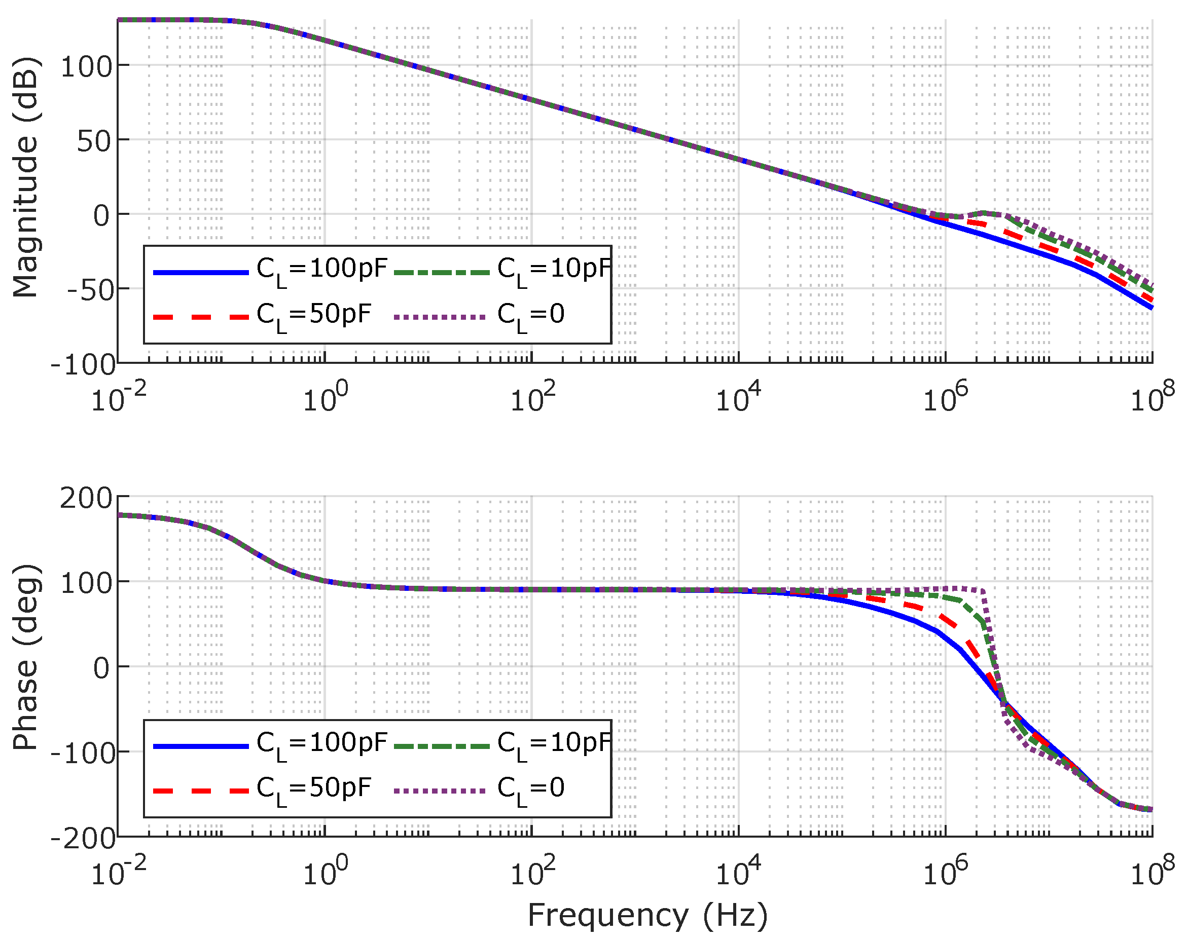
Figure 6. A consistent phase margin above 53° for all
values ensures the stability of the regulator.
2.2. Enhancing the Dynamic Response
To further enhance the dynamic performance without compromising power efficiency, a simple time response enhancement circuit (TREC) is incorporated. The circuit uses a dynamic path only active during transients and minimizes the need for additional components.
Figure 2 depicts the TREC circuitry for both overshoot and undershoot enhancement. The TREC that activates when an undershoot occurs consists of a PMOS QFG transistor
and an NMOS current mirror
–
. The gate voltage of
is set to
via the resistor
, so that in steady state
remains in the cut-off region because
V
. Meanwhile, when a sudden load current increase causes
to decrease, this undershoot is coupled to the gate of
by
= 0.8 pF, thus turning
on. The resulting current is mirrored by
–
(3 μm/0.34 μm, 6 μm/0.34 μm) and injected to the gate of
, which helps restore the output voltage and mitigates the undershoot. Once
stabilizes to its nominal value,
–
revert to the off state.
As for the portion of the TREC that activates when an overshoot occurs, it consists of a single QFG NMOS transistor , which remains off during steady state. The DC gate voltage is set to V through the large value resistance . A sudden reduction in the load current produces an increase in the gate voltage of the pass transistor, which is coupled by to the gate of , thus turning it on and establishing a discharge pathway at the output node. Once reverts to its nominal value, deactivates. Note that, for test purposes, the bias voltages and are externally generated.
In
Figure 7, the TREC behavior is evaluated under full load current transitions from 0–50 mA with 1 μs rise/fall time. At
= 1.9 V, without the TREC, a load change induces an undershoot of 315 mV and an overshoot of 120 mV. The incorporation of the TREC modulates these transients and reduces the undershoot to 182 mV and the overshoot to 106 mV. Furthermore, the overshoot settling time is reduced from 11 to 2 μs.
3. Post-Layout Results
The proposed LDO regulator was designed in the UMC 0.18 μm CMOS process with 3.3 V nominal MOS transistors (
= −0.72 V,
= 0.59 V) to deliver an output regulated voltage
= 1.8 V for
= 1.9 V–3 V and load currents 0–50 mA, with
up to 100 pF. The
is externally set to 1.2 V, and the total quiescent current is 13.8 μA. The layout is shown in
Figure 8, with a total area consumption of 314 μm × 150 μm. The main post-layout simulation results reported next were obtained using Spectre with a BSIM3v3 level 53 transistor model.
3.1. Static Performance
Figure 9 shows the DC characteristic
(
) −
for different load currents and over different process corners: FF, SS, FnSp, and SnFp. The regulator presents a stable 1.8 V output voltage with a 100 mV dropout voltage.
Figure 10 shows the line regulation (LNR =
) over all of the input voltage range (from 1.9 V to 3.0V) at different
values and different process corners. Notably, the LNR is 27 μV/V (TT) and 30 μV/V (SS) at
= 50 mA, which corresponds to the worst case.
Figure 11 depicts the load regulation performance (LDR =
) over the whole
range and for different process corners with
= 1.9 V (worst case scenario). For a load current range of 0–50 mA, the LDR is 1.4 μV/mA in the nominal case (TT) and 4 μV/mA in the worst case (SS).
3.2. Dynamic Performance
Figure 12 presents the response of the proposed LDO for a full load transient 50 mA–0–50 mA, with 1 μs edge time, at
= 1.9 V and
= 100 pF. Thanks to the TREC block, with minimum current and area penalty, the overshoot and undershoot remain below 106 mV and 182 mV, respectively, with 2.03 μs recovery time measured at 99% of the final output voltage value.
Figure 13 shows the response of the LDO regulator when the edge time is reduced to 100 ns. In this case, the maximum overshoot and undershoot were 97 mV and 222 mV, respectively, and the recovery time at 99% of the final output voltage is below 1.64 μs.
3.3. Comparison
Table 2 summarizes and compares the performance of the proposed LDO regulator with other recent topologies with similar specifications. To better evaluate and compare them, several figures of merit (FOMs) were adopted. The first FOM considers the impact of the edge time,
, a parameter that affects the regulator’s response time [
8]. To do so, an edge time factor,
K, is used, defined by the equation:
is then defined as:
The second
evaluates the dynamic performance taking into account a correction factor,
:
where
is given by:
and
represents the minimum load current of the proposed regulator, which is related to its stability. Thus,
accounts for the regulator’s stability under minimum operating current conditions.
Finally, the third
[
25] considers the power efficiency, as well as the regulation performance (LNR and LDR), and is defined as:
The factor 1000 is included to adjust the units (fs). Note that, for all the considered FOMs, the lower the value, the better the performance they showcase.
From the results in
Table 2, it is clear that the proposed LDO design features a broader input voltage range (
= 1.9–3 V) and a lower dropout voltage (
= 100 mV) making it suitable for a variety of regulation applications.
Additionally, the proposed LDO regulator excels in and , which are 0.55 ns and 0.001 fs, respectively, the lowest among the compared works. These values indicate an excellent trade-off between power efficiency ( = 13.8 μA), regulation represented by the low values of LNR (0.027 mV/V) and LDR (0.0014 mV/mA), and dynamic performance, highlighted by a short settling time ( = 2.03 μs). Furthermore, in contrast to some state-of-the-art regulators, the proposed LDO is capable of operating across the entire range of load currents ( = 0–50 mA), indicating an overall enhanced trade-off between power efficiency, dynamic response, and stability across the entire range of loads.


