Article

Effect of In-Situ H Doping on the Electrical Properties of In2O3 Thin-Film Transistors

1
State Key Laboratory Base of Novel Functional Materials and Preparation Science, School of Materials Science and Chemical Engineering, Ningbo University, Ningbo 315211, China
2
Laboratory of Advanced Nano Materials and Devices, Ningbo Institute of Materials Technology and Engineering, Chinese Academy of Sciences, Ningbo 315201, China
*
Authors to whom correspondence should be addressed.
Electronics 2024, 13(8), 1478; https://doi.org/10.3390/electronics13081478
Submission received: 14 March 2024 / Revised: 9 April 2024 / Accepted: 11 April 2024 / Published: 13 April 2024
(This article belongs to the Special Issue Feature Papers in Semiconductor Devices)

Abstract

:
In this article, this research demonstrates the influence of in-situ introduction of H2 into the working gas on the physical properties of post-annealed In2O3 thin films and the performance of associated devices. A gradual increase in the H2 ratio leads to improved film quality, as indicated by spectroscopic ellipsometry, X-ray photoelectron spectroscopy, and atomic force microscope analyses showing a reduction in defect states such as band-tail states and VO in the film, and a smoother surface morphology with the root mean square roughness approximately 0.446 nm. Furthermore, this hydrogen doping effect results in a distinct shift in the device’s threshold voltage toward the positive direction, and an improvement in the field-effect mobility and subthreshold swing. Consequently, a high-performance In2O3:H TFT is developed, exhibiting a field-effect mobility of 47.8 cm2/Vs, threshold voltage of −4.1 V and subthreshold swing of 0.25 V/dec. These findings highlight the potential of in-situ H doping as a promising approach to regulate In2O3-based TFTs.

1. Introduction

Since the report by Nomura et al. on thin-film transistors (TFTs) using InGaO3(ZnO)5, oxide semiconductors (OSs) have been extensively researched due to their promising properties, such as wide band gap, excellent electrical properties, simple preparation, and good compatibility with Si-based manufacture. OSs have emerged as exceptional candidates for TFTs in pixel switching/driving applications for flat-panel displays (FPDs) [1]. However, while driving ultra-high-resolution FPDs at high frame rates, the field-effect mobility (μFE) of oxide TFTs needs to be improved further [2]. In addition, other properties such as threshold voltage (Vth) and TFT stability are also critical factors that should be considered simultaneously [3]. Hence, it is essential to explore new OSs or fabrication techniques to improve the performance of OS TFTs.
Prototype OS materials used in TFT devices are indium oxide (In2O3), tin oxide (SnO2), and zinc oxide (ZnO). Among them, In2O3-based OSs are considered as the most promising materials to achieve high mobility. Firstly, the conduction band bottom of In2O3 is composed of the 5s orbitals of the indium ion with a large orbital radius and a high overlap, which provides a highway for electron transportation [4,5]. Secondly, theoretical calculations show that In2O3 has a small and isotropic effective mass of electrons (0.22 m0) [6]. Finally, some theories suggested that a higher In content results in a larger average effective coordination number of M–O bonds and more corner-, edge-, and face-shared M–O polyhedrons, which enhances overlapping of electron wavefunctions [3]. However, the excessively high carrier concentration (generally larger than 1018 cm−3) of In2O3 makes it challenging to adjust electrical properties [4,7]. In order to regulate the electrical performance of In2O3-based TFTs, researchers have been studying extensively the effect of doping, which is considered to be the most promising method due to its effectiveness and simplicity.
Dopants can be categorized into cation and anion elements. In the case of cation doping, dopants with elements such as Ti, Hf, Zr, Bi, and W that have high oxygen bond dissociation energies, suppressed the concentration of excess oxygen vacancies (VO), and then reduced the electron concentration in the films and improved the stability of the device [8,9,10,11,12]. Doping with lanthanide elements, such as Pr and Tb, shortened the relaxation time of photo-generated electrons and then enhanced the device’s stability [13,14]. However, it should be noted that those cation dopants tend to have a somewhat degrading effect on the μFE of TFTs. On the other hand, anionic dopants like N, F, and H were also introduced to tune the film and the device’s performance. It was found that nitrogen doping could enhance the device’s stability by suppressing VO and other trap states [15,16], while fluoride could passivate VO, suppress the formation of free carriers, and then improve stability [17,18,19]. And there are also a few reports on hydrogen doping. Wardenga et al. prepared H-doped In2O3 thin films (In2O3:H) by RF magnetron sputtering and found that hydrogen passivation of grain boundaries was the main reason for the high mobility observed in In2O3:H films [20]. Magari et al. conducted a study on anion doping with H and found that it plays a crucial role in increasing grain size and decreasing subgap defects, leading to an enhanced μFE [21]. In summary, it mainly contributed the μFE improvement to H-induced grain growth. Therefore, it is essential to further investigate H doping in In2O3, to supply more information on its effect on the film and device properties, such as the film microstructure, device μFE, device threshold voltage (Vth), and others.
In this work, In2O3 and In2O3:H films were deposited by magnetron sputtering and their physical properties were investigated as a function of the H2 ratio in the working gas. The results show that increasing the introduction of H2 induces no grain growth, widens the band gap, makes the absorption edge steeper, and increases the percentage of M-O bonds. These variations correspond to a clear reduction in the electron concentration in In2O3. As a result, the TFT Vth obviously shifts to the positive direction and the μFE is also improved with increasing H2 ratio, showing that H doping is a promising way to regulate In2O3-based TFTs.

2. Experimental Methods

Heavily p-type doped Si wafers and 100 nm-thick SiO2 were utilized as the gate electrode and insulator, respectively. The 25 nm In2O3 and In2O3:H channels were deposited using a 2-inch diameter In2O3 ceramic target (99.99% purity) through RF magnetron sputtering in a mixture of Ar, O2, and H2 gases at room temperature (RT). The O2 and H2 gas flow ratios are denoted as R[O2] = O2/(Ar + O2 + H2) and R[H2] = H2/(Ar + O2 + H2), respectively. For the In2O3 and In2O3:H film, R[O2] was constant at 2.5%, R[H2] was set to 0, 3, and 5%. The films were annealed at 350 °C for 1 h in air, and then a 100 nm-thick Al source/drain (S/D) layer was deposited through the direct current (DC) magnetron sputtering method using pure Ar gas at an input power of 65 W. The In2O3 and Al films were patterned using two different shadow masks. The width/length (W/L) was 800 μm/400 μm. Finally, the fabricated TFTs were annealed at 250 °C for 1 h in air. The optical absorption coefficient of the films was obtained through spectroscopic ellipsometry analysis (SE, M-2000 DI, J. A. Woollam, Lincoln, NE, USA), and the films’ structural changes and crystallinity were evaluated via X-ray diffraction (XRD, D8 ADVANCE DAVINCI, Bruker, Karlsruhe, DE, USA) and transmission electron microscopy (TEM, Talos F200X, Thermo Fisher, Waltham, MA, USA). Surface morphology of the films was observed using an atomic force microscope (AFM, Dimension ICON, Bruker, Billerica, MA, USA). Hall effect testing was employed to determine various electrical properties of the thin films (8404-CRX-6.5K, Lake Shore, Woburn, MA, USA), whereas X-ray photoelectron spectroscopy (XPS, AXIS ULTRA DLD, Shimadzu, Kyoto, Japan) was utilized to investigate internal properties and bonding character. A Keithley 4200SCS semiconductor parameter analyzer was employed to determine the electrical characteristics of the TFT devices.

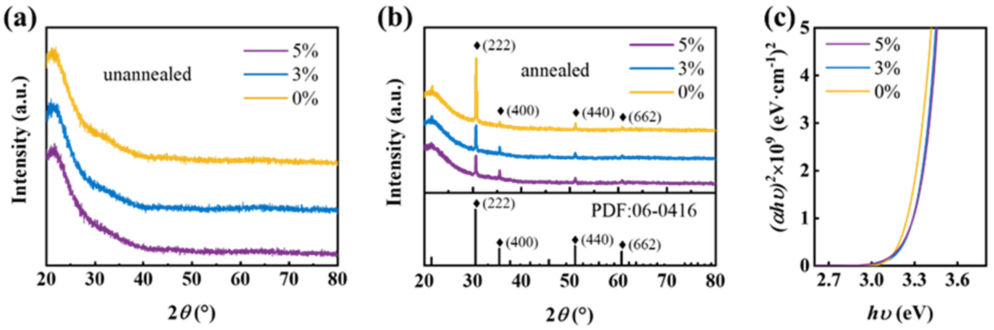
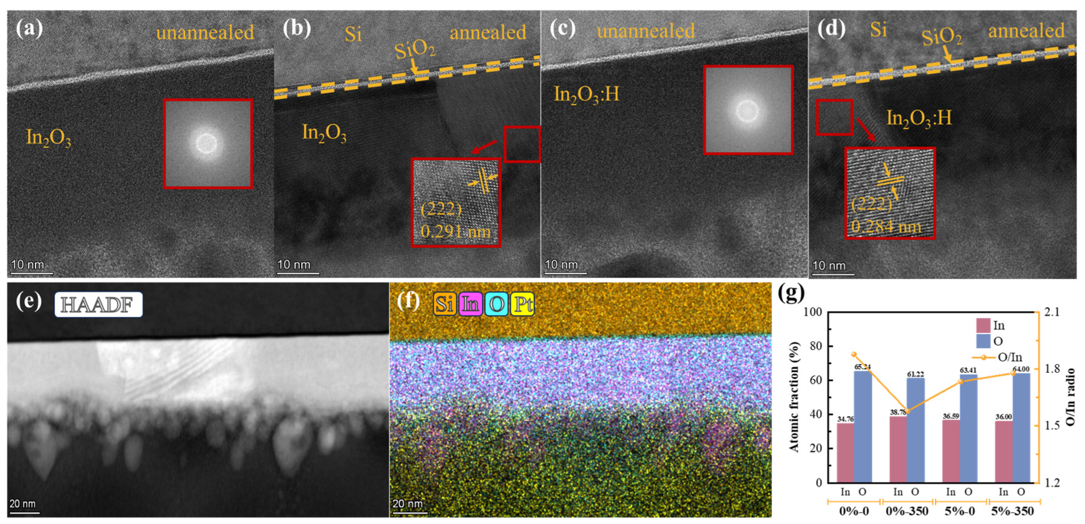
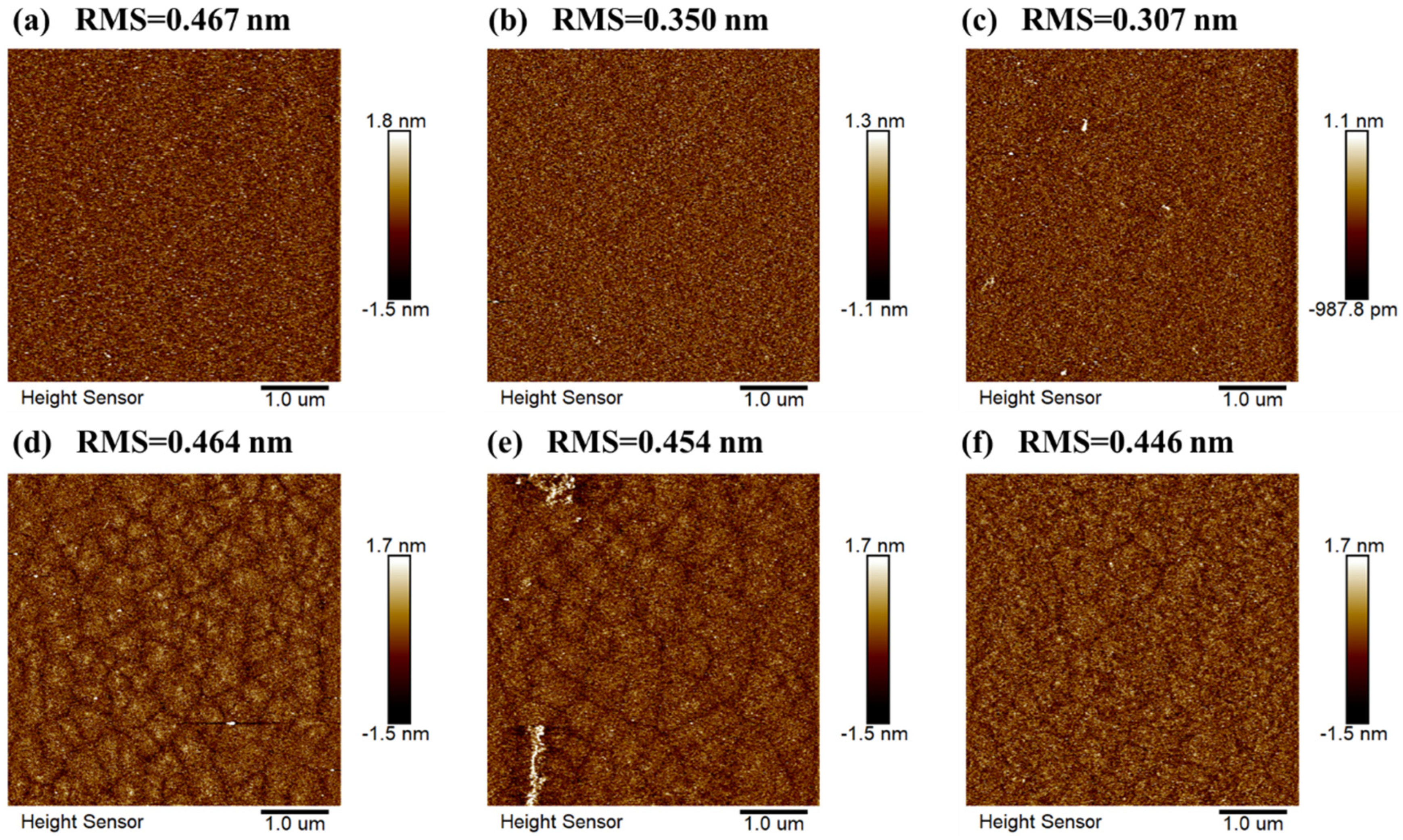
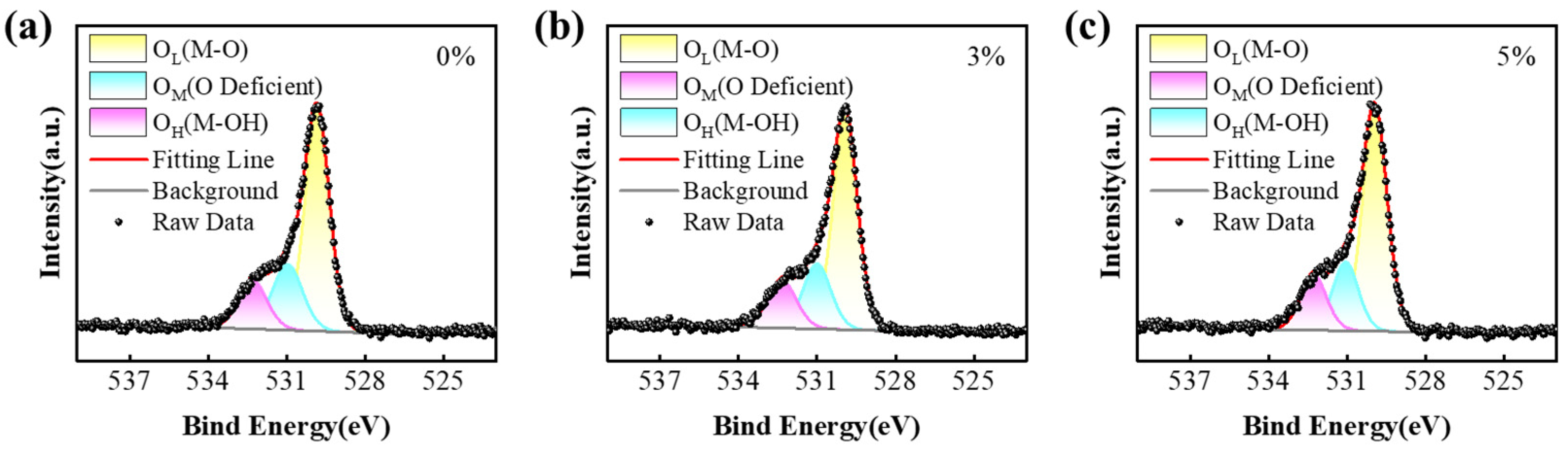
3. Results and Discussion

Figure 1a displays the XRD patterns in θ-2θ scans of 50 nm-thick unannealed In2O3 films with varying R[H2]. The XRD spectra of as-deposited In2O3 films presented low diffraction intensity and rather broad background, indicating that the as-deposited films produced through magnetron sputtering are amorphous. After annealing in air at 350 °C for 1 h, all the films turn to the polycrystalline state; as observed in Figure 1b, there are four clear characteristic peaks which correspond to the (222), (400), (440), and (622) crystal planes [22]. These observed diffraction lines agree well with the cubic bixbyite indium oxide structure (JCPDS06-0416) and Ia-3 space group (Number: 206). Calculated with Scherrer’s formula on the reflection (222), the grain sizes of the In2O3 films with 0%, 3%, and 5% hydrogen content are determined to be 50.6 nm, 48.2 nm, and 49.5 nm, respectively. Interestingly, as R[H2] increases, the intensity of the (222) peak gradually lowers. These results indicate that the introduction of H in In2O3 does not promote grain growth, while it even more or less suppresses the crystallinity [23]. It is worth mentioning that these observations diverge from existing reports on H-doped In2O3 [21], which may be attributed to the discrepancy in the phases of the as-deposited In2O3 films: polycrystalline in the literature and amorphous in this work.
Figure 1c presents the optical band gap (Eg) of the annealed films, which is estimated by the Tacu method (α~(hν−Eg)n) [24]. Since In2O3 has a direct band gap [25], then n = ½ and thus is estimated by extrapolating the linear (αhν)2 edge, where represents the incident photon energy and α is the absorption coefficient obtained by spectroscopic ellipsometry analysis. The optical band gaps of In2O3 thin films are mostly reported in the range of 2.9–3.8 eV [7,23,25,26,27,28]. The calculated Eg values of the In2O3:H films are very similar: about 3.28 eV, which is slightly larger than that of the In2O3 film (3.23 eV). And it can be observed that the absorption edges of the In2O3:H films are clearly steeper than that of the In2O3 film. These imply that the addition of hydrogen may be able to reduce the band-tail defects in In2O3, although it decreases the crystallinity of the In2O3 film.
In order to verify the crystallinity of the film, four representative samples were selected as undoped In2O3 and In2O3:H films with the highest doping concentration (R[H2] = 5%) in the as-deposited and annealed states, respectively. The cross-sectional HR-TEM images of the four representative samples are presented in Figure 2a–d. For the as-deposited samples, the films exhibit an amorphous structure, consistent with the Fast Fourier Transformed results (inserts in Figure 2a,c), revealing diffused hollow rings indicative of the amorphous phase. Upon annealing, distinct grain boundaries and diffraction stripes were observed in Figure 2b,d. The domain-spacing (d-spacing) of the two labeled spherical particles in the (222) crystal plane is about 2.91 and 2.84 Å, respectively, which is consistent with the standard cubic bixbyite-type structure of In2O3 (JCPDS06-0416). These results are in line with the results from the XRD test.
Figure 2e exhibits the high-angle angular dark-field (HAADF) image of In2O3:H films (R[H2] = 5%); the interface between the Si layer and In2O3 layer is distinct and sharp. The thickness of the In2O3 layer is measured to be approximately 47.8 nm. This result is in good agreement with the simulated thickness which obtains from the spectroscopic ellipsometry analysis. One may also observe some large particles at the Pt region, which makes the In2O3/Pt interface unclear. These particles can be observed on all the samples chosen for TEM testing. Figure S1a shows the HAADF image of the as-deposited In2O3:H films at R[H2] = 5%, where the particles are larger and their details are clearer compared to Figure 2c. EDS element analysis, shown in Figure S1b, shows that the element distribution of these large particles is indium-rich and oxygen-poor, which is the opposite of the element content inside the film. The atomic fractions (%) of Pt, O, and In are 2.78%, 25.89%, and 71.33%, respectively. By combining the two figures, it can be clearly observed that those large particles are separated from the indium oxide film region, seemingly suspended on the surface of this sample. This is because there is a distinct boundary between the particles and the In2O3 region, and the boundary is dominated with Pt. Figure 2f illustrates the corresponding energy-dispersive spectrometer (EDS) mapping for Si, In, O, and Pt elements, which reveals the homogeneous distribution of all elements. The In and O elements in the representative sample film were analyzed and the O/In ratio was calculated, as shown in Figure 2g. The results indicate minimal variation in the content of In and O across all samples. The O/In ratios of the hydrogen-doped films exhibit minimal change before and after annealing, in stark contrast to the undoped films. For the undoped films, upon thermal annealing at 350 °C, both the O content and the O/In ratios decrease and the VO increase, implying that some O atoms escape from their lattice positions, which is a frequent reported phenomenon for metal oxide semiconductors [29,30,31]. Conversely, in the case of H-doped films, the O/In ratios remain statistically unchanged between the as-deposited and annealed states. It is suggested that the introduction of hydrogen during the sputtering process may be the underlying cause of this phenomenon, as it significantly enhances the films’ ability to fix oxygen. It has been mentioned in the literature that as the temperature increases, the unstable interfacial In-H-In defects release hydrogen, which in turn combines with oxygen to form stronger covalent bonds, such as In-OH [32,33]. Furthermore, the O/In ratios of the annealed In2O3 film are observed to be lower than that of the annealed In2O3:H film.
Figure 3 shows the topographic profiles obtained by AFM scanning on both the as-deposited and annealed films at different hydrogen concentrations. A high-pass filter was applied to remove the swelling component on the substrate. The root mean square (RMS) roughness calculated from the AFM image is also displayed in Figure 3. The RMS values of the as-deposited films with hydrogen concentration of 0%, 3%, and 5% are 0.467, 0.350, and 0.307 nm, respectively. Notably, the test results reveal a gradual reduction in roughness with the introduction of hydrogen during the deposition process. After thermal annealing at 350 °C, the images showed that the surface morphology of In2O3 and In2O3:H thin films had undergone significant alterations, aligning well with the findings derived from XRD analysis. During the annealing process, the grains gradually aggregate to form grain clusters, and obvious boundaries are formed around the clusters. And the surface morphology of the undoped In2O3 film after annealing bears resemblance to the texture of a Hami melon peel. Compared with the annealed In2O3 film, the boundary surrounding the crystal clusters in the In2O3:H films becomes shallower, and the surface is notably smoother.
To further investigate the effect of hydrogen, XPS measurements were conducted. Considering that water, carbon, and other impurity molecules in the air will be adsorbed onto and even into the sample, a high dose of argon ions, specifically with an ion energy of 2 KeV and a current density of roughly 5 μA/cm2, was applied to sputter away the top surface layer (about 20 nm), while the total thickness of the sample was 50 nm. Figure 4a–c shows the O 1s spectra for the inner layer of the annealed films. They are calibrated by taking the binding energy of the C 1s peak (284.8 eV) as a reference. Gaussian fitting is employed to deconvolute the O 1s peaks. The lowest binding energy Gaussian peak (OL) at 529.8 eV originates from metal–oxygen bonds (M-O lattice); the peak at the middle binding energy 530.7 eV (OM) is linked to O2− ions of oxygen defects, such as VO; while the highest binding energy Gaussian peak (OH) at 531.9 eV is usually associated with specific chemisorbed oxygen such as –CO3, –OH, and H2O [34,35,36]. The area percentages of the three O peaks were calculated and are summarized in Table 1. It was found that with increasing R[H2], the percentage of M-O bonds (OL) increases while the recent part related to the defects and impurities (OM and OH) decreases. This implies that in-situ H doping in the deposition of In2O3 film aids in improving film quality during the post-annealing process, especially by reducing VO or other impurity defects. It is also consistent with the EDS element content analysis that the In2O3:H film has less VO than the In2O3 film, which has higher oxygen content and a higher O/In ratio.
To investigate the electrical properties of the annealed In2O3 and In2O3:H films, Hall effect measurement was employed to determine the Carrier Hall mobility (μH), electron concentration (Ne), and resistivity (ρ) of the thin films. The summarized data are presented in Table 1. The undoped film exhibits a low ρ (0.586 Ω∙cm) and a relatively high Ne of 7.46 × 10¹⁷/cm3. Upon the introduction of H, the ρ increases by at least one order of magnitude, which mainly originates the decrease in the Ne, down to 4.64 × 10¹⁶/cm3 at R[H2] = 3% and 6.53 × 10¹⁶/cm3 at R[H2] = 5%. Additionally, the μH increased from 14.3 cm2/Vs for the In2O3 film to 18.0 cm2/Vs for the In2O3:H film. These variations imply that there are fewer donor defects available to provide free electrons in the In2O3:H films compared to the undoped In2O3 film. These findings also agree well with the results obtained from absorption spectra and XPS analysis that VO and band-tail states are clearly reduced by H doping, since these two kinds of defects are highly associated with donor states near the conduction band minimum of OSs. And the reduction in these defect states also brings an increase in mobility due to the reduction in carrier scattering centers. In addition, a smoother surface morphology also plays a role in improving the mobility of the device.
The fabricated In2O3-based TFTs’ device structure is depicted in Figure 5a. The transfer characteristics of all annealed TFTs, displayed in Figure 5b, were measured at room temperature with a drain-source voltage (VDS) of 10.1 V. Vth was defined by gate voltage (VGS) at a drain current (ID) of 10 nA, and SS was extracted from VGS, which required an increase in the ID average values from 0.1 nA to 10 nA. It is evident that as the R[H2] gradually increases, the Vth of the TFTs significantly shifts toward the positive direction. Specifically, the Vth changes from −15.0 V to −4.1 V. This observed shift in Vth corresponds well with the decrease in Ne of the films, as determined by the Hall measurement. What is more, the μFE of the device also exhibits an improvement trend with increasing R[H2]. Herein, the μFE is derived from the transfer curves measured at VDS = 10.1 V, where the devices are working in the saturation region (as seen in the output curves of Figure 5c). The μFE values increase from 37.8 cm2/Vs to 47.8 cm2/Vs, which is in good accordance with the corresponding trend observed for the μH. It is worth noting that the μFE values are larger than the μH values due to the special carrier transportation mechanism corresponding to the percolation theory for OSs [37]. In TFTs, as the gate voltage increases, localized states become occupied with gate-induced carriers, causing the Fermi level (EF) to shift toward the mobility edge (Em). In such scenarios, the occupied localized states do not trap additional electrons. Particularly when the gate-induced carriers occupy a significant portion of the localized states and the electron density in the channel is sufficiently high to elevate the EF above Em, electrons can move more freely, resulting in higher mobility compared to intrinsic films with lower Ne. As a result, the electrons can move relatively freely, leading to a higher mobility compared to the intrinsic films with lower Ne. Figure 5c shows the output characteristics of In2O3 (R[H2] = 0%), In2O3:H (R[H2] = 3%), and In2O3:H (R[H2] = 5%) devices. The ID increases linearly at the region of low source-drain voltage (VDS), indicating that an Ohmic contact formed between the S/D electrodes and channel layer. Clear pinch-off and saturation characteristics are evident in the saturation region of the output curve, indicating effective control of the transistor channel by the gate and source/drain. In2O3:H TFTs all exhibit high levels of output curve saturation current (VDS = 15 V, ID = 587 μA@VGS = 15 V at R[H2] = 3%, ID = 560 μA@VGS = 12 V at R[H2] = 5%). The ID of In2O3 TFT without introducing H2 is decreased to 361 μA (VGS = 1 V, VDS = 15 V). It shows that with the addition of hydrogen, the TFT exhibits excellent current amplification performance.
In addition, as depicted in Figure 5b and detailed in Table 2, the off-state current (Ioff) of the device subjected to the in-situ hydrogen doping process is significantly lower compared to that of the undoped device. As a result, the on–off current ratio (Ion/Ioff) of the device shows a notable improvement, increasing specifically from 2.83 × 10⁷ (R[H2] = 0%) to 7.20 × 10⁸ (R[H2] = 5%), where the Ion refers to the current value at VGS = 15 V on the transfer curve. These improvements can sensitively reflect changes in the channel defect states. It is worth noting that there is a distinct improvement in subthreshold swing (SS) from 0.52 V/dec to 0.25 V/dec after in-situ H doping. The SS is generally considered as an indicator of the sum of the defect states in oxide semiconductors and semiconductor/dielectric interface trap states. In this context, we introduce the concept of an effective maximum areal density of states, denoted as Neff, which is calculated using the following formula [38]:
N e f f = S S log e k T q 1 C o x q
where k represents the Boltzmann constant, T is the temperature, q is the electron charge, and Cox denotes gate oxide capacitance per unit area. The Neff were calculated to be 1.82 × 10¹², 9.46 × 10¹¹, and 8.76 × 1011 cm−2/eV for In2O3 TFTs deposited at R[H2] = 5%, 3%, and 0%, respectively. These results indicate that an increase in R[H2] leads to a reduction in the Neff of the device. Since the dielectrics and fabrication conditions used are the same just with H doping, it is believed that the semiconductor/dielectric interface trap states are very similar for the three devices, and the decrease in the Neff should correspond to the reduction in the defect states in oxide semiconductors: this is more strong proof that the film quality of In2O3 can be improved via in-situ H doping in as-deposited films.

4. Conclusions

In summary, polycrystalline In2O3 thin films and transistor devices were fabricated by room temperature magnetron sputtering with the introduction of H2 into the working gas following an air annealing. Compared to the undoped one, the H-doped thin films show fewer defects (including oxygen vacancies and band-tail states) and a smoother surface morphology with similar average grain sizes. And the electron concentration obtained by Hall effect testing in the In2O3:H films is approximately one order of magnitude lower than that in the undoped films, while the Hall mobility is enhanced. Regarding thin-film transistors, the threshold voltage gradually shifts toward the positive direction and the field-effect mobility increases with an increase in H2 ratio, agreeing well with the variation trends for the thin films. And the improved subthreshold swing values indicate a reduction in defect states in In2O3:H films. The optimized In2O3:H TFT demonstrates markedly improved electrical performance, including a high field-effect mobility of 47.8 cm2/Vs, a more positive threshold voltage, and a smaller subthreshold swing of 0.25 V/dec. These results supply a comprehensive investigation on the property evolutions for H-doped In2O3 thin films and their TFTs, which would provide an opportunity to boost their further exploration and application.

Supplementary Materials

The following supporting information can be downloaded at: https://www.mdpi.com/article/10.3390/electronics13081478/s1, Figure S1: (a) HAADF image and (b) EDS mapping results of the as-deposited In2O3:H films at R[H2] = 5%.

Author Contributions

Conceptualization, L.L.; Methodology, L.L.; Software, P.H. and L.Y.; Formal analysis, P.H., Z.G. and W.L.; Investigation, Z.G. and X.L.; Data curation, T.L.; Writing—original draft, P.H.; Writing—review & editing, P.H.; Visualization, Y.Q.; Supervision, L.L., Y.H. and H.C.; Funding acquisition, H.C. All authors have read and agreed to the published version of the manuscript.

Funding

This project is supported by the National Key Research and Development Program of China (2021YFB3600701), the National Natural Science Foundation of China (62274167), the Key deployment project of the Chinese Academy of Sciences (ZDRW-XX-2022-2), the Natural Science Foundation of Zhejiang Province (LD21F040002) and the Innovation and Entrepreneurship Team of Zhejiang Province (2021R01003).

Data Availability Statement

Data are contained within the article and Supplementary Materials.

Conflicts of Interest

The authors declare no conflicts of interest.

References

  1. Nomura, K.; Ohta, H.; Ueda, K.; Kamiya, T.; Hirano, M.; Hosono, H. Thin-Film Transistor Fabricated in Single-Crystalline Transparent Oxide Semiconductor. Science 2003, 300, 1269–1272. [Google Scholar] [CrossRef] [PubMed]
  2. Kamiya, T.; Nomura, K.; Hosono, H. Present Status of Amorphous In–Ga–Zn–O Thin-Film Transistors. Sci. Technol. Adv. Mater. 2010, 11, 044305. [Google Scholar] [CrossRef] [PubMed]
  3. Liang, L.; Zhang, H.; Li, T.; Li, W.; Gao, J.; Zhang, H.; Guo, M.; Gao, S.; He, Z.; Liu, F.; et al. Addressing the Conflict between Mobility and Stability in Oxide Thin-Film Transistors. Adv. Sci. 2023, 10, 2300373. [Google Scholar] [CrossRef]
  4. Nomura, K.; Ohta, H.; Takagi, A.; Kamiya, T.; Hirano, M.; Hosono, H. Room-Temperature Fabrication of Transparent Flexible Thin-Film Transistors Using Amorphous Oxide Semiconductors. Nature 2004, 432, 488–492. [Google Scholar] [CrossRef] [PubMed]
  5. Fortunato, E.; Barquinha, P.; Martins, R. Oxide Semiconductor Thin-Film Transistors: A Review of Recent Advances. Adv. Mater. 2012, 24, 2945–2986. [Google Scholar] [CrossRef] [PubMed]
  6. Feneberg, M.; Nixdorf, J.; Lidig, C.; Goldhahn, R.; Galazka, Z.; Bierwagen, O.; Speck, J.S. Many-Electron Effects on the Dielectric Function of Cubic In2O3: Effective Electron Mass, Band Nonparabolicity, Band Gap Renormalization, and Burstein-Moss Shift. Phys. Rev. B. 2016, 93, 045203. [Google Scholar] [CrossRef]
  7. Yu, X.; Zeng, L.; Zhou, N.; Guo, P.; Shi, F.; Buchholz, D.B.; Ma, Q.; Yu, J.; Dravid, V.P.; Chang, R.P.H.; et al. Ultra-Flexible, “Invisible” Thin-Film Transistors Enabled by Amorphous Metal Oxide/Polymer Channel Layer Blends. Adv. Mater. 2015, 27, 2390–2399. [Google Scholar] [CrossRef] [PubMed]
  8. Aikawa, S.; Nabatame, T.; Tsukagoshi, K. Effects of Dopants in InOx-Based Amorphous Oxide Semiconductors for Thin-Film Transistor Applications. Appl. Phys. Lett. 2013, 103, 172105. [Google Scholar] [CrossRef]
  9. Kim, W.-S.; Moon, Y.-K.; Kim, K.-T.; Shin, S.-Y.; Du Ahn, B.; Lee, J.-H.; Park, J.-W. The Influence of Hafnium Doping on Bias Stability in Zinc Oxide Thin Film Transistors. Thin Solid Films 2011, 519, 5161–5164. [Google Scholar] [CrossRef]
  10. Xiao, P.; Dong, T.; Lan, L.; Lin, Z.; Song, W.; Song, E.; Sun, S.; Li, Y.; Gao, P.; Luo, D.; et al. High-Mobility Flexible Thin-Film Transistors with a Low-Temperature Zirconium-Doped Indium Oxide Channel Layer. Phys. Status Solidi-Rapid Res. Lett. 2016, 10, 493–497. [Google Scholar] [CrossRef]
  11. Stewart, K.A.; Gouliouk, V.; Keszler, D.A.; Wager, J.F. Sputtered Boron Indium Oxide Thin-Film Transistors. Solid-State Electron. 2017, 137, 80–84. [Google Scholar] [CrossRef]
  12. Kizu, T.; Aikawa, S.; Mitoma, N.; Shimizu, M.; Gao, X.; Lin, M.-F.; Nabatame, T.; Tsukagoshi, K. Low-Temperature Processable Amorphous In-W-O Thin-Film Transistors with High Mobility and Stability. Appl. Phys. Lett. 2014, 104, 152103. [Google Scholar] [CrossRef]
  13. Zhang, H.; Liang, L.; Wang, X.; Wu, Z.; Cao, H. Praseodymium-Doped In-Sn-Zn-O TFTs with Effective Improvement of Negative-Bias Illumination Stress Stability. IEEE Trans. Electron. Devices 2022, 69, 152–155. [Google Scholar] [CrossRef]
  14. Lan, L.; Li, X.; Ding, C.; Chen, S.; Su, H.; Huang, B.; Chen, B.; Zhou, H.; Peng, J. The Effect of the Charge Transfer Transition of the Tetravalent Terbium on the Photostability of Oxide Thin-Film Transistors. Adv. Electron. Mater. 2022, 8, 2200187. [Google Scholar] [CrossRef]
  15. Liu, P.-T.; Chou, Y.-T.; Teng, L.-F.; Li, F.-H.; Shieh, H.-P. Nitrogenated Amorphous InGaZnO Thin Film Transistor. Appl. Phys. Lett. 2011, 98, 052102. [Google Scholar] [CrossRef]
  16. Li, J.; Fu, Y.-Z.; Huang, C.-X.; Zhang, J.-H.; Jiang, X.-Y.; Zhang, Z.-L. Nitrogen Anion Doping as a Strategy to Suppress Negative Gate-Bias Illumination Instability of ZnSnO Thin Film Transistor. Appl. Phys. Lett. 2016, 108, 143505. [Google Scholar] [CrossRef]
  17. Zhang, J.; Charnas, A.; Lin, Z.; Zheng, D.; Zhang, Z.; Liao, P.-Y.; Zemlyanov, D.; Ye, P.D. Fluorine-Passivated In2O3 Thin Film Transistors with Improved Electrical Performance via Low-Temperature CF4/N2O Plasma. Appl. Phys. Lett. 2022, 121, 172101. [Google Scholar] [CrossRef]
  18. Kim, H.-D.; Kim, J.H.; Park, K.; Kim, J.H.; Park, J.; Kim, Y.J.; Kim, H.-S. Effects of Fluorine Doping on the Electrical Performance of ZnON Thin-Film Transistors. ACS Appl. Mater. Interfaces 2017, 9, 24688–24695. [Google Scholar] [CrossRef] [PubMed]
  19. Kim, H.-D.; Naqi, M.; Jang, S.C.; Park, J.-M.; Park, Y.C.; Park, K.; Nahm, H.-H.; Kim, S.; Kim, H.-S. Nonvolatile High-Speed Switching Zn-O-N Thin-Film Transistors with a Bilayer Structure. ACS Appl. Mater. Interfaces 2022, 14, 13490–13498. [Google Scholar] [CrossRef]
  20. Wardenga, H.; Frischbier, M.; Morales-Masis, M.; Klein, A. In Situ Hall Effect Monitoring of Vacuum Annealing of In2O3:H Thin Films. Materials 2015, 8, 561–574. [Google Scholar] [CrossRef]
  21. Magari, Y.; Kataoka, T.; Yeh, W.; Furuta, M. High-Mobility Hydrogenated Polycrystalline In2O3 (In2O3:H) Thin-Film Transistors. Nat. Commun. 2022, 13, 1078. [Google Scholar] [CrossRef] [PubMed]
  22. Ge, C.; Liu, Z.; Zhu, Y.; Zhou, Y.; Jiang, B.; Zhu, J.; Yang, X.; Zhu, Y.; Yan, S.; Hu, H.; et al. Insight into the High Mobility and Stability of In2O3:H Film. Small 2023, 20, 2304721. [Google Scholar] [CrossRef] [PubMed]
  23. Koida, T. Amorphous and Crystalline In2O3-Based Transparent Conducting Films for Photovoltaics. Phys. Status Solidi A-Appl. Mater. 2017, 214, 1600464. [Google Scholar] [CrossRef]
  24. Catalán, S.; Álvarez-Fraga, L.; Salas, E.; Ramírez-Jiménez, R.; Rodriguez-Palomo, A.; de Andrés, A.; Prieto, C. Charge Mobility Increase in Indium-Molybdenum Oxide Thin Films by Hydrogen Doping. Appl. Surf. Sci. 2016, 386, 427–433. [Google Scholar] [CrossRef]
  25. Weiher, R.L.; Ley, R.P. Optical Properties of Indium Oxide. J. Appl. Phys. 1966, 37, 299–302. [Google Scholar] [CrossRef]
  26. Girtan, M.; Rusu, G.I.; Rusu, G.G.; Gurlui, S. Influence of Oxidation Conditions on the Properties of Indium Oxide Thin Films. Appl. Surf. Sci. 2000, 162, 492–498. [Google Scholar] [CrossRef]
  27. Addonizio, M.L.; Spadoni, A.; Antonaia, A.; Usatii, I.; Bobeico, E. Hydrogen-Doped In2O3 for Silicon Heterojunction Solar Cells: Identification of a Critical Threshold for Water Content and Rf Sputtering Power. Sol. Energy Mater. Sol. Cells 2021, 220, 110844. [Google Scholar] [CrossRef]
  28. Krishna, B.R.; Subramanyam, T.K.; Naidu, B.S.; Uthanna, S. Effect of Substrate Temperature on the Electrical and Optical Properties of Dc Reactive Magnetron Sputtered Indium Oxide Films. Opt. Mater. 2000, 15, 217–224. [Google Scholar] [CrossRef]
  29. Guo, S.; Diyatmika, W.; Unutulmazsoy, Y.; Yang, L.; Dai, B.; Xu, L.; Han, J.; Ralchenko, V.; Anders, A.; Zhu, J. High-Quality Transparent Conductive Indium Oxide Film Deposition by Reactive Pulsed Magnetron Sputtering: Determining the Limits of Substrate Heating. Appl. Surf. Sci. 2022, 585, 152604. [Google Scholar] [CrossRef]
  30. Zhang, C.; Liu, G.; Geng, X.; Wu, K.; Debliquy, M. Metal Oxide Semiconductors with Highly Concentrated Oxygen Vacancies for Gas Sensing Materials: A Review. Sens. Actuators A-Phys. 2020, 309, 112026. [Google Scholar] [CrossRef]
  31. Marwoto, P.; Khanifah, L.; Astuti, B.; Wibowo, E. Influence of Annealing Time on the Morphology and Oxygen Content of ZnO:Ga Thin Films. J. Phys. Conf. Ser. 2019, 1321, 022020. [Google Scholar] [CrossRef]
  32. Medvedeva, J.E.; Sharma, K.; Bhattarai, B.; Bertoni, M.I. Hydrogen Behavior at Crystalline/Amorphous Interface of Transparent Oxide Semiconductor and Its Effects on Carrier Transport and Crystallization. ACS Appl. Mater. Interfaces 2022, 14, 39535–39547. [Google Scholar] [CrossRef] [PubMed]
  33. Shi, J.; Zhang, J.; Yang, L.; Qu, M.; Qi, D.-C.; Zhang, K.H.L. Wide Bandgap Oxide Semiconductors: From Materials Physics to Optoelectronic Devices. Adv. Mater. 2021, 33, 2006230. [Google Scholar] [CrossRef] [PubMed]
  34. He, J.; Li, G.; Lv, Y.; Wang, C.; Liu, C.; Li, J.; Flandre, D.; Chen, H.; Guo, T.; Liao, L. Defect Self-Compensation for High-Mobility Bilayer InGaZnO/In2O3 Thin-Film Transistor. Adv. Electron. Mater. 2019, 5, 1900125. [Google Scholar] [CrossRef]
  35. Wang, H.; He, J.; Xu, Y.; Andre, N.; Zeng, Y.; Flandre, D.; Liao, L.; Li, G. Impact of Hydrogen Dopant Incorporation on InGaZnO, ZnO and In2O3 Thin Film Transistors. Phys. Chem. Chem. Phys. 2020, 22, 1591–1597. [Google Scholar] [CrossRef]
  36. Li, W.; Yang, L.; Gao, Z.; Ren, J.; Hu, P.; Li, T.; Liang, L.; Cao, H. Impact of the Source/Drain Electrode Process on the Mobility-Threshold Trade-Off for InSnZnO Thin-Film Transistors. ACS Appl. Electron. Mater. 2023, 5, 1615–1619. [Google Scholar] [CrossRef]
  37. Kamiya, T.; Nomura, K.; Hosono, H. Electronic Structures Above Mobility Edges in Crystalline and Amorphous In-Ga-Zn-O: Percolation Conduction Examined by Analytical Model. J. Disp. Technol. 2009, 5, 462–467. [Google Scholar] [CrossRef]
  38. Nakata, M.; Zhao, C.; Kanicki, J. DC Sputtered Amorphous In–Sn–Zn–O Thin-Film Transistors: Electrical Properties and Stability. Solid-State Electron. 2016, 116, 22–29. [Google Scholar] [CrossRef]
Figure 1. XRD patterns of the In2O3 and In2O3:H films deposited at different R[H2] and at a constant R[O2] value of 2.5% (a) before and (b) after annealing at 350 °C in air. Inset: (bottom) standard XRD spectra of In2O3. (c) Plots of (αhν)2 versus of the annealed In2O3 and In2O3:H films.
Electronics 13 01478 g001
Figure 2. Cross-sectional HR-TEM images (a) 0%-0, (b) 0%-350, (c) 5%-0, (d) 5%-350. The insets to (a,c) show the Fast Fourier Transformed images of the as-deposited films. (e) HAADF image and (f) EDS mapping results of the annealed In2O3:H films at R[H2] = 5%. (g) Atomic fractions of In, O, and the O/In radios in as-deposited and annealed In2O3 and In2O3:H films obtained from EDS analysis.
Electronics 13 01478 g002
Figure 3. AFM images and root mean square roughness RMS (a) 0%-0, (b) 3%-0, (c) 5%-0, (d) 0%-350, (e) 3%-350, (f) 5%-350.
Electronics 13 01478 g003
Figure 4. The XPS O 1s spectroscopic analysis of In2O3 etching films at a depth of 20 nm with different R[H2]: (a) R[H2] = 0%; (b) R[H2] = 3%; (c) R[H2] = 5%.
Electronics 13 01478 g004
Figure 5. (a) Schematic view of a TFT device. (b) Typical transfer characteristics (VDS = 10.1 V) for all devices with In2O3 and In2O3:H channels deposited at various R[H2] values. (c) Typical output curves of the TFTs.
Electronics 13 01478 g005
Table 1. The percentage of O 1s peak area in XPS spectra and Hall effect testing results of the films.
In-O
(%)
VO
(%)
Impurity Molecules (%)μH
(cm2/Vs)
Ne
(1/cm3)
ρ
(Ω∙cm)
0%61.3220.4618.2214.37.46 × 10170.586
3%62.6819.7417.5918.04.64 × 10167.49
5%63.9518.7617.2918.06.53 × 10165.31
Table 2. The main electrical parameters and derived effective defect density of states for TFT devices.
Vth (V)μFE (cm2/Vs)Ion/IoffSS (V/dec)Neff (cm−2/eV)
0%-350−15.037.82.83 × 1070.521.82 × 1012
3%-350−5.245.65.94 × 1080.279.46 × 1011
5%-350−4.147.87.20 × 1080.258.76 × 1011
Disclaimer/Publisher’s Note: The statements, opinions and data contained in all publications are solely those of the individual author(s) and contributor(s) and not of MDPI and/or the editor(s). MDPI and/or the editor(s) disclaim responsibility for any injury to people or property resulting from any ideas, methods, instructions or products referred to in the content.

