Article

Characteristics Analysis of IGZO TFT and Logic Unit in the Temperature Range of 8–475 K

1
Institute of Microelectronics of the Chinese Academy of Sciences, Beijing 100029, China
2
School of Microelectronics, University of Chinese Academy of Sciences, Beijing 100049, China
3
School of Microelectronics, Guizhou Normal University, Guiyang 550025, China
4
Beijing Zhongke Newmicro Technology Co., Ltd., Beijing 100029, China
*
Authors to whom correspondence should be addressed.
Electronics 2024, 13(8), 1427; https://doi.org/10.3390/electronics13081427
Submission received: 29 February 2024 / Revised: 2 April 2024 / Accepted: 6 April 2024 / Published: 10 April 2024

Abstract

:
The effect of high- and low-temperature conditions on the performance of IGZO TFT and logic circuits were investigated in this work. In the temperature range of 250−350 K, the performance of the IGZO TFT did not show significant changes and exhibited a certain degree of high- and low-temperature resistance. When the temperature was below 250 K, as the temperature decreased, the threshold voltage (VTH) of the IGZO TFT significantly increased, the field effect mobility (μFE) and the on state current (ION) significantly decreased. This is attributed to the lower excitation degree of charge carriers at extremely low temperatures, resulting in fewer charge carriers transitioning to the conduction or valence bands, and the formation of defects also limits carrier migration. When the temperature exceeded 350 K, as the temperature increased, more electrons could escape from the bandgap trap state and become free charge carriers, and the IGZO layer was thermally excited to produce more oxygen vacancies, resulting in higher μFE and lower VTH. In addition, the drain current noise spectral density of IGZO TFT conformed to the 1/ƒ noise characteristic, and the degradation mechanism of IGZO TFT over a wide temperature range was confirmed based on the changes in noise spectral density at different temperatures. In addition, an inverter logic unit circuit was designed based on IGZO TFT, and the performance changes over a wide temperature range were analyzed. This lays the foundation for IGZO TFT to be applied in integrated circuits with harsh environments.

1. Introduction

In recent years, amorphous indium–gallium–zinc oxide (a-IGZO) thin-film transistor (TFT) has been widely used in various fields such as displays, sensors, memory, and neural morphology systems due to its unique advantages in off-state leakage current, carrier mobility, threshold voltage, and manufacturing process [1,2,3,4,5]. In addition, a-IGZO TFT has broad application prospects in the field of monolithic 3-D (M3D)-integrated circuits due to its high compatibility with complementary metal oxide semiconductors (CMOS), wide bandgap (Eg~3.05 eV), and excellent manufacturing yield characteristics [6,7,8,9]. Furthermore, considering that the electron conduction path in IGZO is mainly formed by the extended spherical 5s orbitals of In3+, the overlap between the 5s wave functions of adjacent In3+ is not sensitive to the disordered local structure of a-IGZO,s making IGZO TFT a potential device for applications in harsh environments [10,11].
Given the current promising development potential of IGZO TFTs in many fields, and with the push towards employing circuits fabricated in the latest technology for space and military environments, it is necessary to evaluate the performance changes of IGZO TFTs in extreme environments [12]. Current research indicates that amorphous materials have a more flexible atomic bond structure compared to crystalline silicon, and their structural plasticity leads to easy defect reconstruction, with the potential to achieve large-scale scalable radiation resistance [13]. The research on the radiation effects of IGZO TFT for space applications is also actively advancing, and preliminary results have been achieved [14,15,16,17,18,19,20]. In addition, the stable operating temperature range of commercial integrated circuits (ICs) is usually between 25–85 °C (298–358 K). However, with the development of aerospace, gas, down-hole oil, and other fields, the performance of semiconductor devices and circuits in higher- or lower-temperature ranges is facing enormous challenges [21]. In order to comprehensively explore the potential of IGZO TFT for harsh environmental applications, it is necessary to study the performance changes of IGZO TFT and related circuits over a wide temperature range. At present, there has been research progress on IGZO TFT under high-temperature conditions, and the device exhibits strong temperature dependence under high-temperature conditions [22,23]. However, the degradation mechanism of IGZO TFT and related logic unit circuits over a wide temperature range is currently unclear.
In this work, IGZO TFT devices with good electrical performance were prepared using radio frequency (RF) magnetron sputtering technology. The inverter unit circuit was designed based on IGZO TFT. The influence of temperature on the electrical performance of IGZO TFT and an inverter circuit was studied within a wide temperature range of 8–475 K, and the degradation mechanism of the device was analyzed based on the relationship between key electrical parameters and temperature. This study aims to provide reference for promoting the application of IGZO TFT and related circuits in harsh environments.

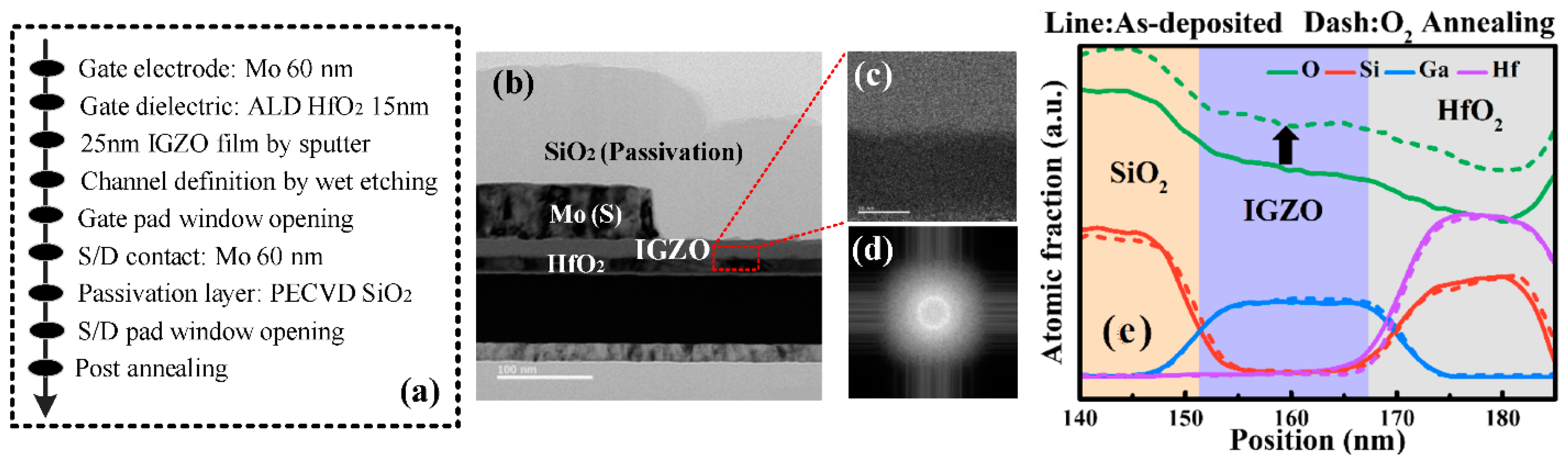
2. Devices and Methods

The IGZO TFTs were fabricated using a backed-gate process on the 8-inch pilot CMOS line at the Institute of Microelectronics of the Chinese Academy of Sciences. For the device fabrication, a 200 nm SiO2 buffer layer was deposited on a silicon substrate through plasma-enhanced chemical vapor deposition (PECVD). Subsequently, 60 nm thick Mo layer was sputtered and subjected to dry etching to form a bottom gate electrode. HfO2 with a thickness of 15 nm was deposited as a gate insulator layer (GI) using the PECVD method. Then, a 25 nm thick a-IGZO film was deposited and patterned using radio frequency magnetron sputtering technology in an Ar/O2 atmosphere at room temperature. The atomic ratio of the IGZO film was In:Ga:Zn = 1:1:1, the sputtering power was 200 W, and the pressure was 1 mTorr. Mo with a thickness of 60 nm was sputtered and patterned to form the source and drain electrodes, and a 100 nm thick SiO2 passivation layer was deposited using the PECVD method. Finally, a-IGZO TFT devices were prepared by high-temperature annealing treatment for 1 hour in a N2 atmosphere at 350 °C to improve their electrical properties. The key process steps for IGZO TFT device manufacturing are shown in Figure 1a.
The transmission electron microscope (TEM) image was obtained by using a focused ion beam (FIB) to cut the cross-section of the device along the channel length direction, as shown in Figure 1b, where each layer of device structure can be clearly observed. Figure 1c shows high-resolution transmission electron microscopy (HRTEM) image, and the relatively clear and sharp interface on the IGZO/HfO2 film indicates good film quality. Figure 1d shows the fast Fourier transform (FFT), which exhibits typical diffuse ring characteristics, indicating that IGZO is amorphous. The elemental composition of IGZO TFT was analyzed using an energy dispersive spectrometer (EDS), as shown in Figure 1e. After O2 annealing, the elemental densities of Si, Ga, and Hf remained basically unchanged, but the O concentration in the a-IGZO channel increased, indicating oxygen permeation and possible filling of oxygen vacancies during the O2 treatment process, which helps to improve the quality of the IGZO thin film.
The gate width (W) and length (L) of the IGZO TFT used are 2 μm and 0.5 μm, respectively. The low-temperature test was conducted in the Institute of Physical Chemistry Technology, Chinese Academy of Sciences, and the low-temperature test was controlled and adjusted within the range of 8–300 K through Lake Shore CRX. The high-temperature test was performed on the Cascade SUMMIT 12,000 B semi-automatic probe platform of the Institute of Microelectronics, Chinese Academy of Sciences. The probe platform incorporates a thermal chuck, and its temperature can be controlled through the ESPEC ETC-200 L unit. Measurements were carried out in the range of 300–475 K. In high-temperature testing, the IDVG and IDVD curves of the IGZO TFT were first tested at room temperature (300 K), and then, the temperature was increased in steps of 25 K until 475 K. At each temperature point, the IDVG and IDVD curves of the device were tested. In low-temperature testing, the device performance at room temperature was also initially tested as a reference, and then, the temperature was decreased in steps of 50 K until 10 K. At each temperature point, the IDVG and IDVD curves of the device were tested.

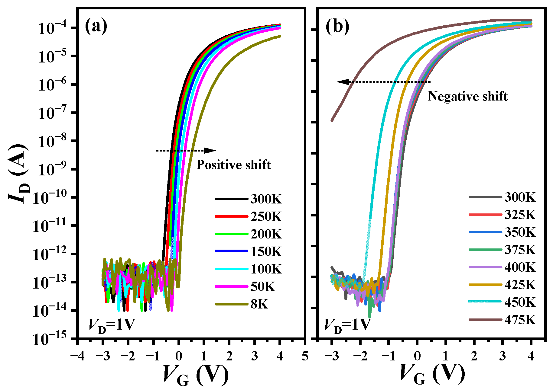
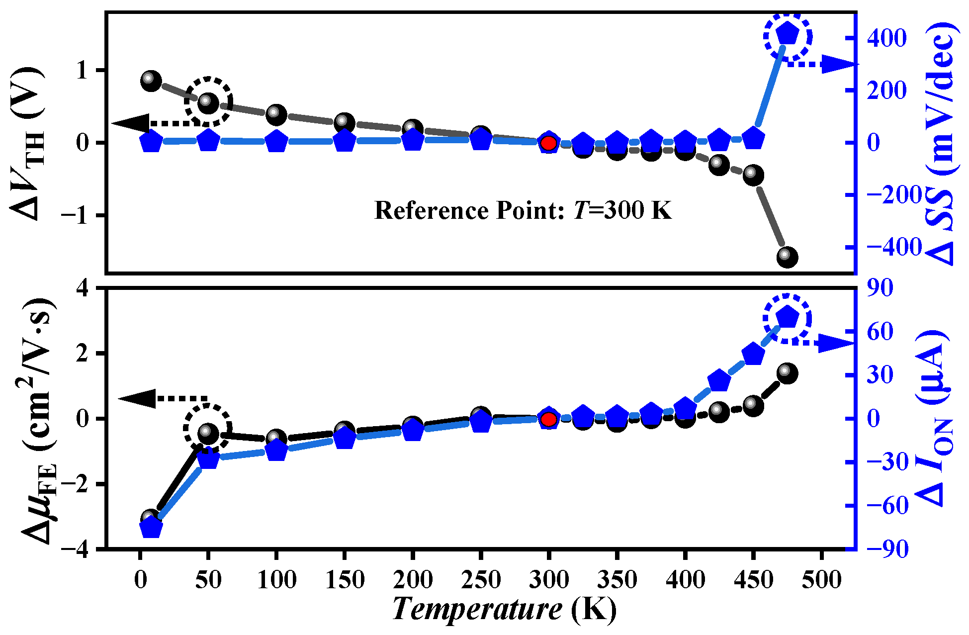
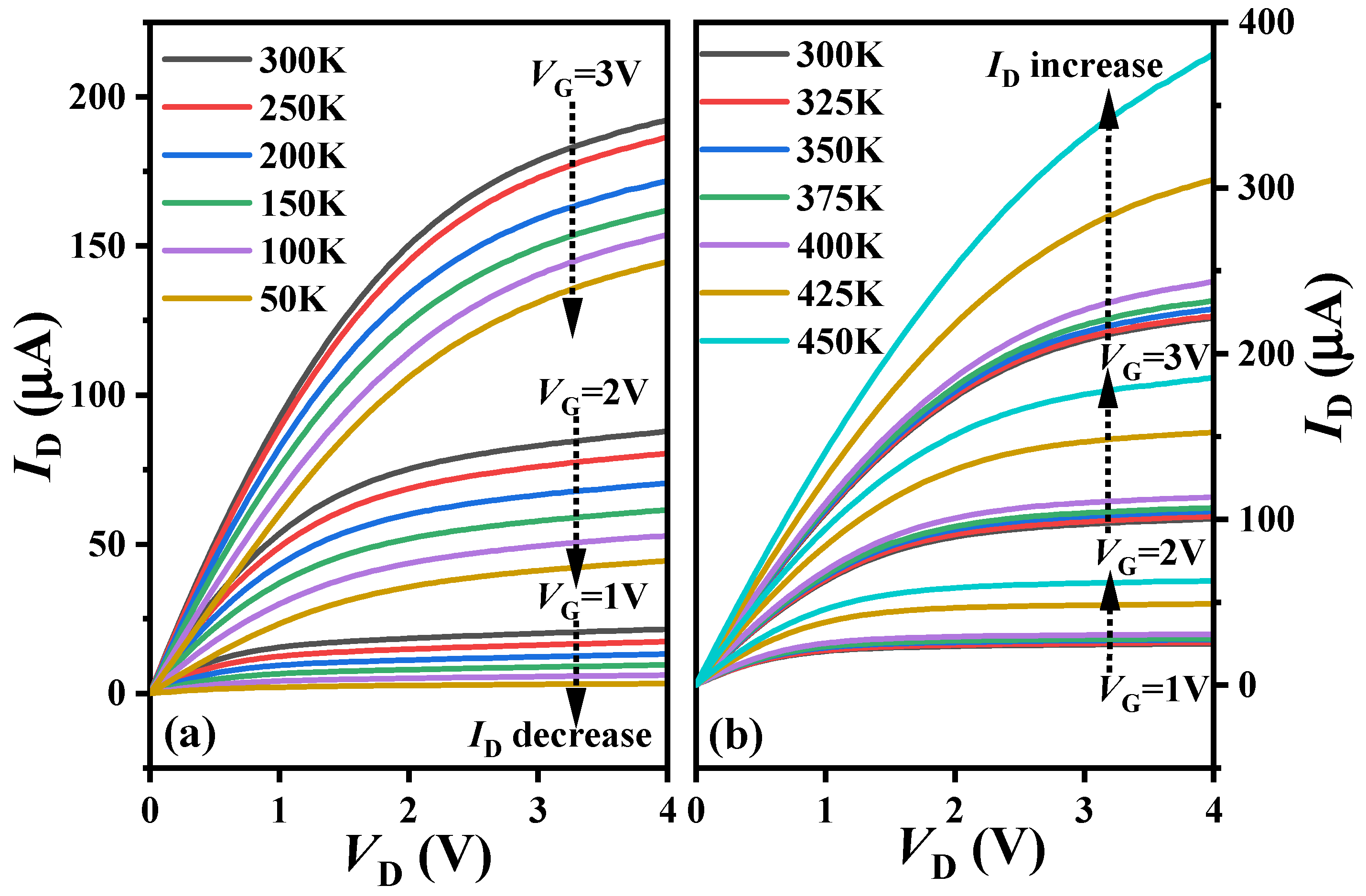
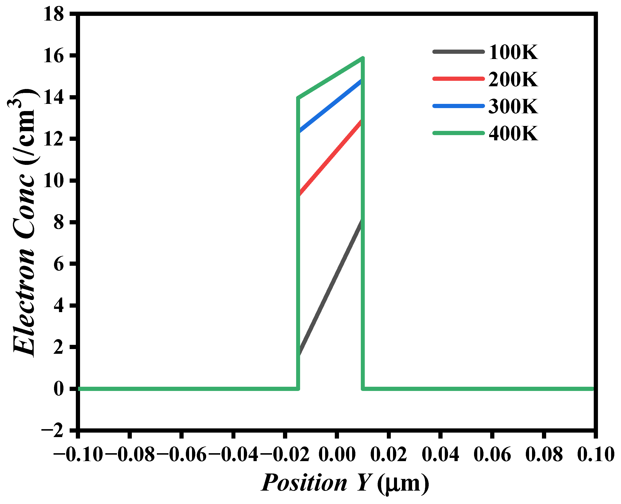
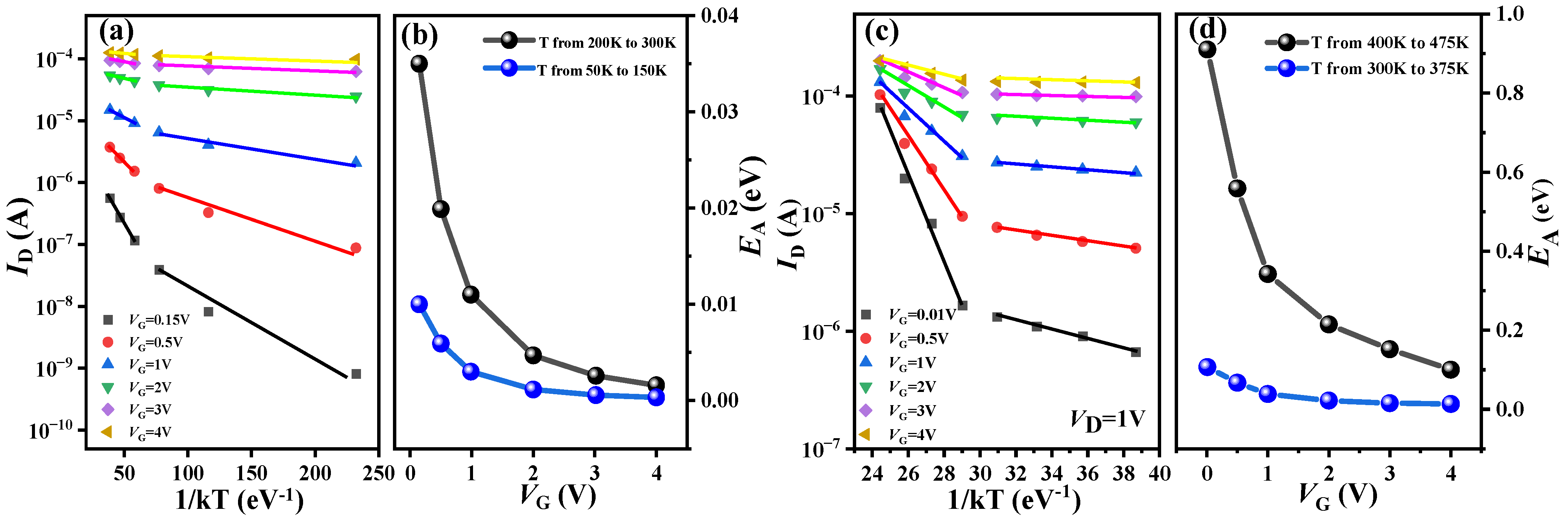
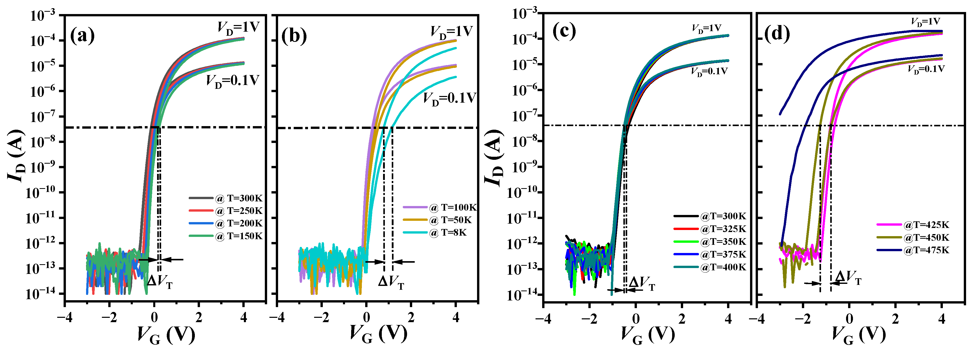
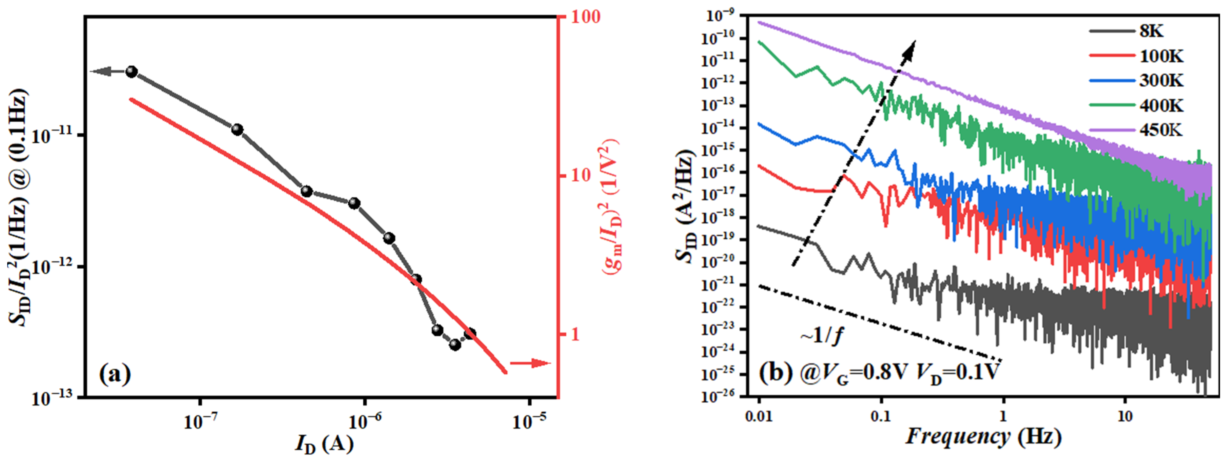
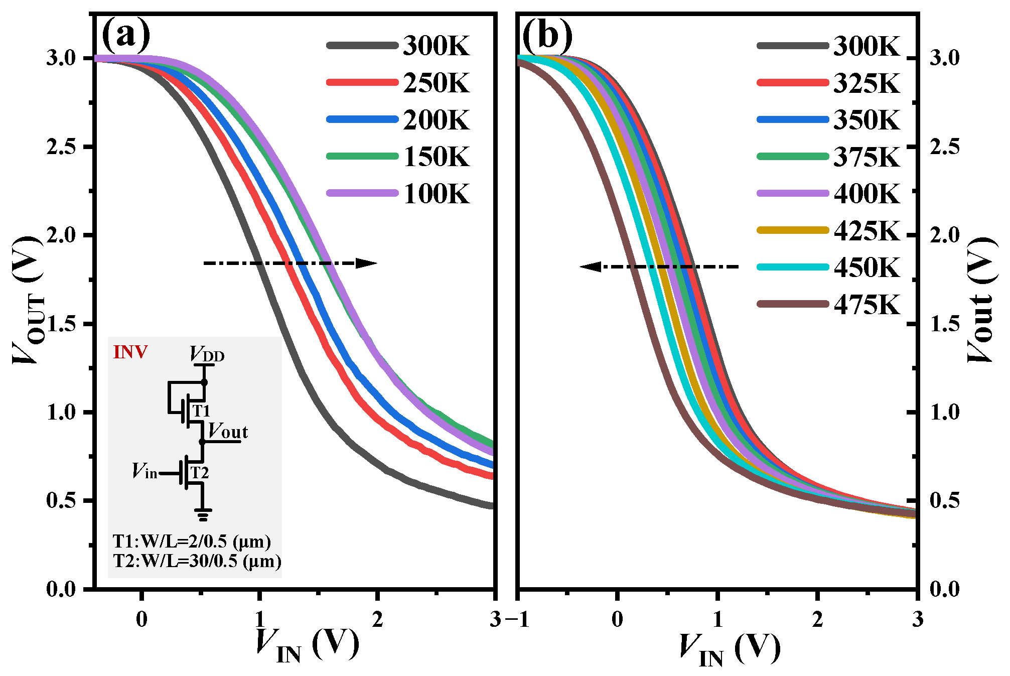
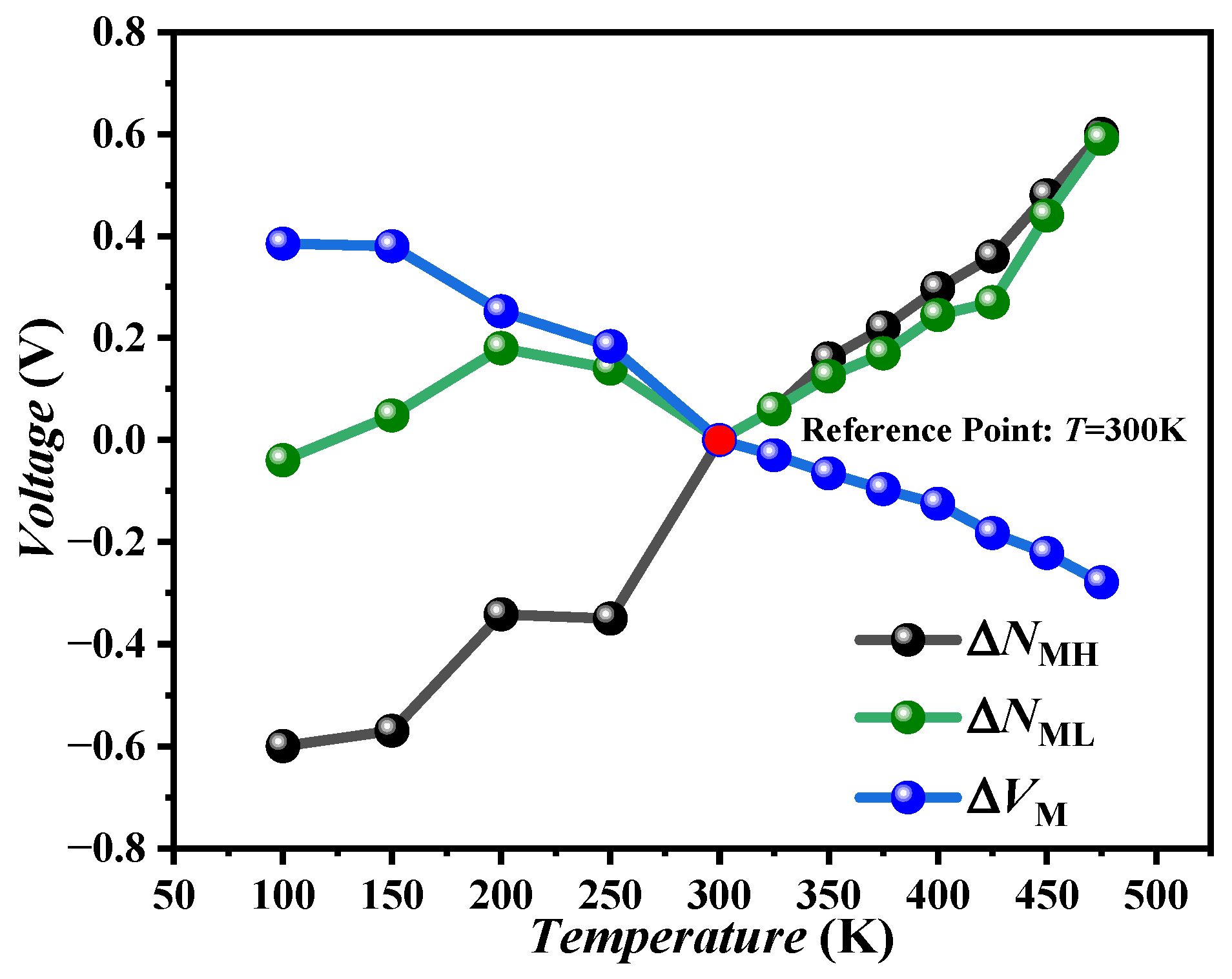
3. Experimental Results and Discussion

The transfer characteristics (IDVG) of a-IGZO TFTs were measured at various temperatures T (from 8 to 475 K) for the gate voltages VG ranging from −3 to 4 V with a fixed drain voltage VD = 1 V, as shown in Figure 2. In the low-temperature range of 8–300 K, the IDVG curve shows a positive shift with the temperature decreases, while in the high-temperature range of 300–475 K, the IDVG curve shows a negative shift with the temperature increases. When the temperature reaches 475 K, the drain current seriously deviates from the normal value within the measurable voltage range, and the device cannot turn off normally. The gate control ability of the IGZO TFT is severely weakened under high temperature.
The key electrical parameters that affect the static characteristics of IGZO TFT include threshold voltage (VTH), field effect mobility (μFE), subthreshold swing (SS), and current switching ratio (ION/IOFF). The extraction of VTH adopts the constant-current method in this work. The VTH is defined as the particular gate voltage (VG) at which drain current (ID) = 10−8 × (W/L) A [24]. The μFE and SS of IGZO TFT is calculated according to the Equations (1) and (2), respectively, where COX is the gate dielectric capacitance per unit area [25]. COX is calculated by the Equation (3).
μ FE = L W C O X V D S d I D d V G
S S = ( d log ( I D ) d V G ) 1 | max
C O X = ε 0 ε O X t O X
where ε0 is the vacuum dielectric constant, and the value is 8.85 × 10⁻¹⁴ F/cm; εOX is the oxide layer dielectric constant, and the value is 20; tOX is the thickness of the oxide layer, and the value is 15 nm. These parameters are inputted into the Equation (4), it can be calculated COX = 1.18 × 10⁻⁶ F/cm2.
Key parameters that characterize the electrical performance of IGZO TFT are extracted according to the IDVG curves at various temperatures in Figure 2, including ΔVTH, ΔSS, ΔμFE, and ΔION. The variation of each parameter with temperature is shown in Figure 3. These parameters are all based on 300 K as a reference point. Taking ΔVTH as an example, ΔVTH represents the difference between the threshold voltage at a specific temperature and the threshold at room temperature, as shown in Equation (4).
Δ V T H = V T H @ T V T H @ 300 K
Figure 3 shows that there is no significant change in the key electrical parameters of the IGZO TFT within the temperature range of 250–350 K, indicating that the device exhibits a certain degree of high- and low-temperature resistance.
When the temperature is below 250 K, as the temperature decreases, the VTH of the IGZO TFT significantly increases, and the μFE and ION significantly decrease. This is attributed to the lower excitation degree of charge carriers at extremely low temperatures, resulting in fewer charge carriers transitioning to the conduction or valence bands, and the formation of defects also limits carrier migration [8,21]. When the temperature exceeds 350 K, as the temperature increases, more electrons can escape from the sub bandgap trap state and become free charge carriers, and the IGZO layer is thermally excited to produce more oxygen vacancies, resulting in larger ION and smaller VTH [22,26]. Therefore, the observed lower VTH with increasing temperature may be due to the combined effect of these free electrons escaping from the sub bandgap trap state together with the generation of oxygen vacancies because of thermal excitation [23,27]. The increase in ΔμFE is also attributed to the increase in thermal energy provided by high temperatures, which increases the kinetic energy of charge carriers and reduces the scattering mechanism that hinders their movement. Furthermore, within the temperature range of 8 K to 450 K, the ΔSS shows a slight increasing trend. When the temperature reaches 475 K, the ΔSS abnormally increases. This may be related to the fact that the oxygen vacancies generated by thermal excitation provide more traps, and charge capture occurs in the gate oxide through thermally assisted tunnelling, leading to an increase in ΔSS [28].
The relationship between the IDVD curves and temperature of a-IGZO TFT is shown in Figure 4. In the low-temperature range, the ID decreases with decreasing temperature; in the high-temperature range, the ID increases with increasing temperature.
The variation relationship between a-IGZO TFT devices and temperature was simulated using TCAD. Specifically, the a-IGZO mobility model related to lattice temperature was used to simulate the changes in device electrical characteristics with temperature. The mobility model was designed to work in conjunction with the defect density model of electronic states [29]. Physical models such as the IGZO.TOKYO temperature model, Shockley–Read–Hall (SRH) generation and recombination, and Fermi statistical model were used in the simulation process [30]. The IDVD curve obtained from TCAD simulation showed a consistent trend with the experimental test results as a function of temperature. Figure 5 shows the variation curve of channel electron concentration with temperature in TCAD simulation. As the temperature increases, the channel electron concentration significantly increases.
Figure 6a,c show the linear temperature dependence of the logarithm of ID and 1/kT under different VG voltages at low and high temperatures, respectively, and satisfies the Arrhenius relationship. The relationship between drain current and temperature is described by the Arrhenius Equation (5) [31,32].
I D S = I D S 0 exp ( E A k T )
where k is the Boltzmann constant, T is the temperature, EA is the active energy, IDS0 is the pre-factor, and EA and IDS0 are gate-voltage-dependent quantities.
The transport of charge carriers in channels is mainly influenced under different temperatures and VG by three transport mechanisms, namely variable range hopping (VRH), trap-limited conduction (TLC), and percolation [33]. Among them, when VG is small, at lower temperatures, carriers in the tail states lack sufficient thermal energy to cross the mobility edge (above a specific energy level near the conduction band minimum), and hence, transport is dominated by carriers undergoing VRH, tunneling between localized tail states, with lower carrier mobility in the channel, resulting in small ID. At higher temperatures, Fermi-level (EF) in the localized tail states and transport is dominated by TLC where carriers are thermally excited from the localized tail states to the extended states above mobility edge, resulting in an increase in carrier mobility and ID compared to low temperatures; when VG is large, as EF efficiently moves above the mobility edge, percolation-dominated transport is observed for all temperatures, with higher carrier mobility in the channel, resulting in large ID.
The activation energy of drain current shows differences in the temperature ranges of 50–150 K, 200–300 K, 300–375 K, and 400–475 K. The activation energy corresponding to different VG in the higher-temperature region is generally higher than that in the lower-temperature region. Specifically, Figure 6b,d summarize the variation curves of activation energy with gate voltage over different temperature ranges. This is because for amorphous semiconductor TFTs, most of the charge induced by the gate electric field goes into the tail states, with a small fraction going into the conduction band [34]. As the gate voltage increases, the movement of EF towards EC leads to a change of the occupancy of the localized state, which in turn leads to a gradual decrease in activation energy [22].
Figure 7 shows the IDVG curves with VD = 0.1 V and VD = 1 V under different temperatures. Usually, the VTH shift in short-channel TFT devices is denoted by drain-induced barrier lowering (DIBL), which originates from the effective lowering of the barrier for current conducting between source and channel [35,36]. To determine the DIBL characteristics, we used the DIBL factor (λDIBL) defined in the Equation (6) [36].
λ D I B L = V T ( @ V D 1 = 0.1 V ) V T ( @ V D 2 = 1 V ) V D 2 V D 1
It is worth noting that when IGZO TFT is exposed to harsh temperature environments, such as temperatures below 150 K and above 425 K, the DIBL effect becomes more severe, as shown in Figure 7b,d. The reason is as follows: At extremely low temperature, the carrier mobility and density decrease, resulting in a more uneven electric field between the gate and channel of the transistor, making it more difficult to control the channel and leading to adverse DIBL effects; at high temperature, the thermally excited oxygen atoms will leave their original positions and generate vacancies as the temperature increases. Oxygen vacancies act as electron donors as VO = VO2+ + 2e [37,38]. The oxygen vacancies near the drain side and source side affect the overall carrier concentration of the active channel. As VD increases, VTH shifts in the negative direction, and the number of thermally excited oxygen atoms increases with temperature, resulting in a more severe DIBL. The ΔλDIBL of IGZO TFT at different temperatures is summarized in Table 1.
In order to analyze the effect of temperature on the charge transfer mechanism of IGZO TFT, the noise characteristics of the device at different temperatures were studied. At room temperature, the normalized drain current noise spectral density (SID/ID2) and the transconductance to drain current squared (gm/ID)2 of IGZO TFT exhibited an approximate trend of variation with drain current, as shown in Figure 8a. Among them, the SID/ID2 was extracted at ƒ = 0.1 Hz for the device. This indicates that the noise spectral density and transconductance of IGZO TFT satisfy the carrier number fluctuation (CNF) theory shown in Equations (7) and (8) [3,39].
S I D I D 2 = ( g m I D ) 2 S V f b
with
S V f b = q 2 N t k T λ W L C o x 2 f
where SVfb is the power spectral density of flat-band voltage fluctuations, Nt is the volume trap density, kT is the thermal energy, λ is the oxide tunneling attenuation distance, WL is the channel area, Cox the gate oxide capacitance per unit area, and f is the frequency [40]. The extracted value of SVfb is 8.9 × 10⁻¹³ V2/Hz for the IGZO TFT device in this work.
The relationship between the drain current noise spectral density and frequency at different temperatures is shown in Figure 8b. The SID of the drain current increases with the increase of temperature, which confirms the degradation mechanism of the active layer of IGZO TFT devices being thermally excited under high-temperature conditions, resulting in an increase in carrier concentration.
The inverter circuit was designed based on the IGZO TFT device, as shown in Figure 9. The transistor T1 with gate drain short circuit is used as the load transistor, T2 is the driving transistor, and the aspect ratios of T1 and T2 are 2/0.5 (μm) and 30/0.5 (μm), respectively. The purpose of using a large-sized T2 is to provide sufficient driving capacity for the inverter to increase output swing. The voltage transmission characteristic (VTC) curve of the inverter was tested at different temperatures and is shown in Figure 8, where the power supply voltage VDD = 3 V. In low-temperature environments, the VTC curve shifts to the right as the temperature decreases; in a high-temperature environment, the VTC curve moves horizontally to the left with the temperature increases. This is consistent with the trends of the IDVG curves of IGZO TFT in Figure 2a,b under low- and high-temperature environments, respectively. This is reasonable because compared to the output drain current of a single transistor, the presence of load transistor T1 in the inverter converts the drain current of transistor T2 into output voltage.
In order to analyze the impact of temperature on the inverter circuit, key parameters affecting inverter performance, such as noise margin values and switching thresholds, were extracted based on the VTC curves at different temperatures. At 300 K, the input low (VIL) and high (VIH) voltage and the output low (VOL) and high (VOH) voltage were extracted from the voltage unit gain points (dVOUT/dVIN = −1), respectively. The specific relationship between the key parameters of the inverter and temperature is shown in Figure 10. Both the high noise margin (NMH = |VOH-VIH|) and low noise margin (NML = |VIL-VOL|) show an increasing trend with the increased temperature [41]. The switching threshold voltage (VM) of the inverter is defined as the point where VIN = VOUT [42]. It is expected that the VM is located near the midpoint of the voltage swing (VDD/2). As shown in Figure 8, it can be seen that the VM shows a decreasing trend with the temperature increasing.

4. Conclusions

In this work, the electrical performance of IGZO TFT devices and related circuits were studied in the wide temperature range of 8–475 K. The experimental results show that within the range of 250–350 K, the IGZO TFT device is less affected by temperature and exhibits high- and low-temperature resistance. When the temperature exceeds this range, the device exhibits a certain degree of performance degradation with the temperature increases or decreases, and the DIBL effect of the device will gradually become significant. When the temperature reaches a high temperature of 475 K, the device cannot turn off normally, indicating that the gate control ability of the device is seriously affected at high temperatures. The 1/ƒ noise characteristics of the device show a significant increase in noise spectral density with increasing temperature, indicating that the IGZO active layer is thermally excited under high-temperature conditions, leading to an increase in carrier concentration. This work provides a reference for the application research of IGZO-based integrated circuits in harsh environments.

Author Contributions

Funding acquisition, J.B. and G.X.; methodology, J.W. and J.B.; software, J.W.; investigation, J.W.; writing—original draft preparation, J.W.; writing—review and editing, J.B.; supervision, M.L. All authors have read and agreed to the published version of the manuscript.

Funding

This research was funded by the State Key Laboratory Special Funding Project of Simulation and Effects of Strong Pulse Radiation Environment (No. SKLIPR2109).

Data Availability Statement

Data are contained within the article.

Acknowledgments

The authors would like to thank all the participants in this study.

Conflicts of Interest

Author Mengxin Liu was employed by the company Beijing Zhongke Newmicro Technology Co., Ltd. The remaining authors declare that the research was conducted in the absence of any commercial or financial relationships that could be construed as a potential conflict of interest.

References

  1. Zhu, Y.; He, Y.L.; Jiang, S.S.; Chen, C.S.; Wan, Q. Indium–gallium–zinc–oxide thin-film transistors: Materials, devices and applications. J. Semicond. 2021, 42, 031101. [Google Scholar] [CrossRef]
  2. Choi, S.; Kim, S.; Jang, J.; Kim, J.; Kim, D.M.; Choi, S.J.; Mo, H.S.; Lee, S.M.; Kim, D.H. Oxygen content and bias influence on amorphous InGaZnO TFT-based temperature sensor performance. IEEE Electron Device Lett. 2019, 40, 1666–1669. [Google Scholar] [CrossRef]
  3. Tang, H.Y.; Li, Y.T.; Sokolovskij, R.; Sacco, L.; Zheng, H.; Ye, H.Y.; Yu, H.Y.; Fan, X.J.; Tian, H.; Ren, T.L.; et al. Ultra-high sensitive NO2 gas sensor based on tunable polarity transport in CVD-WS2/IGZO pn heterojunction. ACS Appl. Mater. Interfaces 2019, 11, 40850–40859. [Google Scholar] [CrossRef] [PubMed]
  4. Bai, Z.H.; Gong, T.Z.; Duan, X.L.; Wang, J.W.; Xiao, K.; Geng, D.; Li, L. Low frequency noise of Channel-All-Around (CAA) InGaZnO field effect transistors. IEEE Electron Device Lett. 2022, 43, 2117–2120. [Google Scholar] [CrossRef]
  5. Liao, C.W. Mobility impact on compensation performance of AMOLED pixel circuit using IGZO TFTs. J. Semicond. 2019, 40, 022403. [Google Scholar] [CrossRef]
  6. Masashi, O.; Yoshinori, A.; Kazuki, T.; Tatsuki, K.; Satoru, O.; Akio, S.; Kunihiro, F.; Shuhei, N.; Tatsuya, O.; Ryota, H.; et al. 3D-Stacked CAAC-In-Ga-Zn oxide FETs with gate length of 72nm. In Proceedings of the IEEE International Electron Devices Meeting (IEDM), San Francisco, CA, USA, 7–11 December 2019; pp. 1950–1953. [Google Scholar]
  7. Kang, Y.Y.; Han, K.Z.; Kumar, A.; Wang, C.K.; Sun, C.; Zhou, Z.P.; Zhou, J.R.; Gong, X. Back-End-of-Line compatible fully depleted CMOS inverters employing Ge p-FETs and a-InGaZnO n-FETs. IEEE Electron Device Lett. 2021, 42, 1488–1491. [Google Scholar] [CrossRef]
  8. Han, K.Z.; Samanta, S.; Xu, S.Q.; Wu, Y.; Gong, X. High field temperature-independent field-effect mobility of amorphous indium-gallium-zinc oxide thin-film transistors: Understanding the importance of equivalent-oxide-thickness downscaling. IEEE Trans. Electron Devices 2021, 68, 118–124. [Google Scholar] [CrossRef]
  9. Kim, M.J.; Park, H.J.; Yoo, S.; Cho, M.H.; Jeong, J.K. Effect of channel thickness on performance of ultra-thin body IGZO field-effect transistors. IEEE Trans. Electron Devices 2022, 69, 2409–2416. [Google Scholar] [CrossRef]
  10. Kamiya, T.; Nomura, K.; Hosono, H. Electronic structure of the amorphous oxide semiconductor a-InGaZnO4–x: Tauc-Lorentz optical model and origins of subgap states. Phys. Status Solidi A 2009, 206, 860–867. [Google Scholar] [CrossRef]
  11. Sheng, J.; Hong, T.; Lee, H.; Kim, K.; Sasase, M.; Kim, J.; Hosono, H.; Park, J.S. Amorphous IGZO TFT with high mobility of ~70 cm2/vs via vertical dimension control using PEALD. ACS Appl. Mater. Interfaces 2019, 43, 40300–40309. [Google Scholar] [CrossRef] [PubMed]
  12. Chatterjee, I.; Zhang, E.X.; Bhuva, B.L. Bias dependence of total-dose effects in bulk FinFETs. IEEE Trans. Nucl. Sci. 2013, 60, 4476–4482. [Google Scholar] [CrossRef]
  13. Ho, D.; Choi, S.; Kang, H. In situ radiation hardness study of amorphous Zn-In-Sn-O thin-film transistors with structural plasticity and defect tolerance. ACS Appl. Mater. Interfaces 2023, 15, 33751–33762. [Google Scholar] [CrossRef] [PubMed]
  14. Costa, J.C.; Pouryazdan, A.; Panidi, J. Flexible IGZO TFTs and their suitability for space applications. IEEE J. Electron Devices Soc. 2019, 7, 1182–1190. [Google Scholar] [CrossRef]
  15. Park, S.; Song, M.K.; Sung, T. Effect of X-ray irradiation on a-IGZO and LTPS thin-film transistors for radiography applications. Appl. Surf. Sci. 2021, 550, 149237. [Google Scholar] [CrossRef]
  16. Kim, D.G.; Kim, J.U.; Lee, J.S. Negative threshold voltage shift in an a-IGZO thin film transistor under X-ray irradiation. RSC Adv. 2019, 9, 20865–20870. [Google Scholar] [CrossRef] [PubMed]
  17. Dayananda, G.K.; Rai, C.S.; Jayarama, A. Simulation model for electron irradiated IGZO thin film transistors. J. Semicond. 2018, 39, 022002. [Google Scholar] [CrossRef]
  18. Pan, C.C.; Yang, S.B.; Chen, L.L. Improvement in bias stability of IGZO TFT with etching stop structure by UV irradiation treatment of active layer island. IEEE J. Electron Devices Soc. 2020, 8, 524–529. [Google Scholar] [CrossRef]
  19. Guo, Z.; Li, K.; Li, X. Total-Ionizing-Dose Effects in IGZO Thin-Film Transistors. IEEE Trans. Nucl. Sci. 2023, 70, 2002–2007. [Google Scholar] [CrossRef]
  20. Dayananda, G.K.; Rai, C.S.; Jayarama, A. Study of radiation resistance property of a-IGZO thin film transistors. In Proceedings of the 2016 IEEE International Conference on Recent Trends in Electronics, Information & Communication Technology (RTEICT), Bangalore, India, 20–21 May 2016; pp. 1816–1819. [Google Scholar]
  21. Wang, H.B.; Bi, J.S.; Bu, J.H.; Liu, H.N.; Zhao, F.Z.; Cao, H.J.; Ai, C. Characteristics of 22 nm UTBB-FDSOI technology with an ultra-wide temperature range. Semicond. Sci. Technol. 2022, 37, 105004. [Google Scholar] [CrossRef]
  22. Estrada, M.; Rivas, M.; Garduño, I.; Avila-Herrera, F.; Cerdeira, A.; Pavanello, M.; Mejia, I.; Quevedo-Lopez, M.A. Temperature dependence of the electrical characteristics up to 370 K of amorphous In-Ga-ZnO thin film transistors. Microelectron. Reliab. 2016, 56, 29–33. [Google Scholar] [CrossRef]
  23. Chang, G.W.; Chang, T.C.; Jhu, J.C.; Tsai, T.M.; Chang, K.C.; Syu, Y.E.; Tai, Y.H.; Jian, F.Y.; Hung, Y.C. Temperature-dependent instability of bias stress in InGaZnO thin-film transistors. IEEE Trans. Electron Devices 2014, 61, 2119–2124. [Google Scholar] [CrossRef]
  24. Yan, G.P.; Yang, H.; Liu, W.B.; Zhou, N.; Hu, Y.P.; Shi, Y.F.; Gao, J.F.; Tian, G.L.; Zhang, Y.D.; Fan, L.J.; et al. Mechanism analysis of ultralow leakage and abnormal instability in InGaZnO thin-film transistor toward DRAM. IEEE Trans. Electron Devices 2022, 69, 2417–2422. [Google Scholar] [CrossRef]
  25. Samanta, S.; Chand, U.; Xu, S.; Han, K.Z.; Wu, Y.; Wang, C.; Kumar, A.; Velluri, H.; Li, Y.; Fong, X.Y.; et al. Low subthreshold swing and high mobility amorphous indium–gallium–zinc-oxide thin-film transistor with thin HfO2 gate dielectric and excellent uniformity. IEEE Electron Device Lett. 2020, 41, 856–859. [Google Scholar] [CrossRef]
  26. Charlene, C.; Katsumi, A.; Hideya, K.; Jerzy, K. Density of states of a-InGaZnO from temperature-dependent field-effect studies. IEEE Trans. Electron Devices 2009, 56, 1177–1183. [Google Scholar]
  27. Takechi, K.; Nakata, M.; Eguchi, T.; Yamaguchi, H.; Kaneko, S. Comparison of ultraviolet photo-field effects between hydrogenated amorphous silicon and amorphous InGaZnO4 thin-film transistors. Jpn. J. Appl. Phys. 2009, 48, 010203. [Google Scholar] [CrossRef]
  28. Durante, O.; Intonti, K.; Viscardi, L. Subthreshold Current Suppression in ReS2 Nanosheet-Based Field-Effect Transistors at High Temperatures. ACS Appl. Nano Mater. 2023, 6, 21663–21670. [Google Scholar] [CrossRef]
  29. Abe, K.; Sato, A.; Takahashi, K.; Kumomi, H.; Kamiya, T.; Hosono, H. Mobility-and temperature-dependent device model for amorphous In–Ga–Zn–O thin-film transistors. Thin Solid Films 2014, 559, 40–43. [Google Scholar] [CrossRef]
  30. Sarkar, A. Device simulation using Silvaco ATLAS tool. In Technology Computer Aided Design; CRC Press: Boca Raton, FL, USA, 2018; pp. 203–252. [Google Scholar]
  31. He, H.Y.; Liu, Y.; Yin, J.L.; Wang, X.L.; Lin, X.N.; Zhang, S.D. Introducing effective temperature into Arrhenius equation with Meyer-Neldel rule for describing both Arrhenius and non-Arrhenius dependent drain current of amorphous InGaZnO TFTs. Solid-State Electron. 2021, 181, 108011. [Google Scholar] [CrossRef]
  32. He, H.; Xiong, C.; Yin, J.L.; Wang, X.L.; Lin, X.N.; Zhang, S.D. Analytical drain current and capacitance model for amorphous InGaZnO TFTs considering temperature characteristics. IEEE Trans. Electron Devices 2020, 67, 3637–3644. [Google Scholar] [CrossRef]
  33. Chakraborty, W.; Ye, H.; Grisafe, B.; Lightcap, I.; Datta, S. Low thermal budget (<250 °C) dual-gate amorphous indium tungsten oxide (IWO) thin-film transistor for monolithic 3-D integration. IEEE Trans. Electron Devices 2020, 67, 5336–5342. [Google Scholar]
  34. Takechi, K.; Nakata, M.; Eguchi, T.; Yamaguchi, H.; Kaneko, S. Temperature-Dependent Transfer Characteristics of Amorphous InGaZnO4 Thin-Film Transistors. Jpn. J. Appl. Phys. 2009, 48, 011301. [Google Scholar] [CrossRef]
  35. Samanta, S.; Han, K.Z.; Sun, C.; Wang, C.K.; Kumar, A.; Thean, A.V.Y.; Gong, X. Amorphous InGaZnO thin-film transistors with sub-10-nm channel thickness and ultra scaled channel length. IEEE Trans. Electron Devices 2021, 68, 1050–1056. [Google Scholar] [CrossRef]
  36. Yang, T.J.; Kim, J.H.; Ryoo, C.I.; Myoung, S.J.; Kim, C.W.; Baeck, J.H.; Bae, J.U.; Noh, J.Y.; Lee, S.W.; Park, K.S.; et al. Analysis of Drain-Induced Barrier Lowering in InGaZnO Thin-Film Transistors. IEEE Trans. Electron Devices 2023, 70, 121–126. [Google Scholar] [CrossRef]
  37. Yang, C.I.; Chang, T.C.; Liao, P.Y.; Chen, L.H.; Chen, B.W.; Chou, W.C.; Chen, G.F.; Lin, S.C.; Yeh, C.Y.; Tsai, C.M.; et al. Drain-Induced-Barrier-Lowing-Like effect induced by oxygen-vacancy in scaling-down via-contact type amorphous InGaZnO thin-film transistors. IEEE J. Electron Devices Soc. 2018, 6, 685–690. [Google Scholar] [CrossRef]
  38. Park, J.S.; Jeong, J.K.; Mo, Y.G.; Kim, H.D. Improvements in the device characteristics of amorphous indium gallium zinc oxide thin-film transistors by Ar plasma treatment. Appl. Phys. Lett. 2007, 90, 262106. [Google Scholar] [CrossRef]
  39. Vodapally, S.; Jang, Y.I.; Kang, I.M.; Cho, I.K.; Lee, J.H.; Bae, Y.; Ghibaudo, G.; Cristoloveanu, S.; Im, K.S.; Lee, J.H. 1/f-Noise in AlGaN/GaN nanowire omega-finfets. IEEE Electron Device Lett. 2016, 38, 252–254. [Google Scholar]
  40. Sindhuri, V.; Son, D.H.; Lee, D.G.; Sakong, S.H.; Jeong, Y.H.; Cho, I.T.; Lee, J.H.; Kim, Y.T.; Cristoloveanu, S.; Bae, Y.H.; et al. 1/f noise characteristics of AlGaN/GaN FinFETs with and without TMAH surface treatment. Microelectron. Eng. 2015, 147, 134–136. [Google Scholar] [CrossRef]
  41. Zhang, Y.; Hu, S.J.; Zhou, Y.F.; Wu, T.W.; Peng, Y.; Deng, H.C.; Bao, X.Q.; Zeng, Q.B. A Two-Dimensional MoS2 device and CMOS inverter based on the plasma immersion doping technique. J. Electron. Mater. 2023, 52, 5218–5226. [Google Scholar] [CrossRef]
  42. Chen, J.B.; Liu, Z.H.; Wang, H.Y.; He, Y.; Zhu, X.X.; Ning, J.; Zhang, J.C.; Hao, Y. A GaN complementary FET inverter with excellent noise margins monolithically integrated with power gate-injection HEMTs. IEEE Trans. Electron Devices 2022, 69, 51–56. [Google Scholar] [CrossRef]
Figure 1. (a) Key fabrication process steps for the fabricated back-gated IGZO TFT devices, (b) cross-section TEM image for the IGZO TFT, (c) partial HRTEM image of the interface between the IGZO layer and HfO2 layer, (d) FFT image, and (e) ESD image for the IGZO TFT.
Electronics 13 01427 g001
Figure 2. (a) The relationship between the IDVG curve and low-temperature changes. The curve shifts in a positive direction with the temperature decreases. (b) The relationship between the IDVG curve and high-temperature changes. The curve shifts in a negative direction with the temperature increases.
Electronics 13 01427 g002
Figure 3. Variation of ΔVTH, ΔSS, ΔμFE, and ΔION extracted from IDVG curves with respect to temperature.
Electronics 13 01427 g003
Figure 4. (a) The relationship between the IDVD curve and low-temperature changes. The ID decreases with the temperature decreases. (b) The relationship between the IDVD curve and high-temperature changes. The ID increases with the temperature increases.
Electronics 13 01427 g004
Figure 5. Channel electron concentration variation with temperature for TCAD simulation.
Electronics 13 01427 g005
Figure 6. (a) The linear low-temperature dependence between the logarithm of ID and 1/kT under different VG voltages; lines are used to extract EA. (b) EA as a function of VG within different low-temperature ranges, (c) the linear high-temperature dependence between the logarithm of ID and 1/kT under different VG voltages. (d) EA as a function of VG within different high-temperature ranges.
Electronics 13 01427 g006
Figure 7. (a) Variation of IDVG curves for IGZO TFT at VD = 0.1V and VD = 1V within the temperature range of 150−300 K; (b) the DIBL effect of IGZO TFT varies with temperature at extremely low temperature; (c) variation of IDVG curves for IGZO TFT at VD = 0.1V and VD = 1V within the temperature range of 300−400 K; (d) the DIBL effect of IGZO TFT varies with temperature at extremely high temperature.
Electronics 13 01427 g007
Figure 8. (a) The SID/ID2 and the (gm/ID)2 as functions of drain current, in which SID/ID2 follows the trend of (gm/ID)2; (b) the relationship between SID and frequency at different temperatures, in which SID shows an increasing trend with the temperature increases.
Electronics 13 01427 g008
Figure 9. (a) The VTC curve of the inverter composed of IGZO TFT varies with low temperature. The inserted diagram is the circuit diagram of the inverter, with T1 as the load transistor and T2 as the drive transistor; (b) the VTC curve of the inverter composed of IGZO TFT varies with high temperature.
Electronics 13 01427 g009
Figure 10. The relationship between the noise margin value of inverters and temperature.
Electronics 13 01427 g010
Table 1. The ΔλDIBL of IGZO TFT varies with temperature.
T (K)ΔλDIBL (mV/V)T (K)ΔλDIBL (mV/V)
8355.532510.52
5075.5350−11.08
10062.5375−10.98
15029.240033.32
20015.5425133.32
25010.5450466.22
3000475>1166.2
Disclaimer/Publisher’s Note: The statements, opinions and data contained in all publications are solely those of the individual author(s) and contributor(s) and not of MDPI and/or the editor(s). MDPI and/or the editor(s) disclaim responsibility for any injury to people or property resulting from any ideas, methods, instructions or products referred to in the content.

