Abstract
LiNbO3 thin films are grown on a c-plane (0001) sapphire wafer at a relatively low substrate temperature by chemical beam vapor deposition (CBVD) in Sybilla equipment. Raman measurements only evidence the LiNbO3 phase, while HR-XRD diffractograms demonstrate a c-axis-oriented growth with only (006) and (0012) planes measured. The rocking curve is symmetric, with a full width at half maximum (FWHM) of 0.04°. The morphology and topography observed by SEM and AFM show very low roughness, with rms equaling 2.0 nm. The optical properties are investigated by a guided-wave technique using prism coupling. The ordinary refractive index (no) and extraordinary refractive index (ne) at different wavelengths totally match with the LiNbO3 bulk, showing the high microstructural quality of the film. The film composition is estimated by Raman and bi-refringence and shows a congruent or near-stoichiometric LiNbO3.
1. Introduction
Lithium niobate (LiNbO3, LN) is an excellent ferroelectric material due to its piezoelectric and electro-optical properties, high Curie temperature (1210 °C), significant resistivity, and high piezo-response. Research regarding the first growth of bulk LiNbO3 crystals by the Czochralski technique [1] was published in 1965, and LiNbO3 is widely used in modulators, resonators and switch manufacturing. However, LiNbO3 bulk has shown its limits in the technology development roadmap, mainly in relation to further device miniaturization and integration as well as difficulties in manufacturing complex architectures (multi-layers, tandem devices, etc.) [2]. The thin film approach is considered as a solution to lift these limits and bottlenecks, in parallel to the ion-slicing technique [3] that enables the production of a high-quality thin-film lithium niobate (TFLN) but presents the drawbacks of high film thickness (>300 nm) and high manufacturing costs. Many techniques have been explored to directly deposit LN thin films (a recent review by B. Zivasatienraj et al. [4]), including sputtering [5,6,7,8,9], sol–gel [10,11,12], vapor transport equilibration (VTE) [13,14], pulsed laser deposition (PLD) [15,16,17], molecular beam epitaxy (MBE) [18,19], Liquid Phase Epitaxy (LPE) [20,21,22] and chemical vapor deposition (CVD) [23,24,25,26,27,28]. Among these, LN films deposited by chemical beam vapor deposition (CBVD) at 650 °C showed very promising results [29,30].
A further challenge remains to grow high-quality LiNbO3 thin films to match the bulk LiNbO3 quality, but also with the required thicknesses, high growth rates and with a process scalable to mass production. Depending on the method, LiNbO3 films can be fabricated at temperatures ranging from 400 °C to over 1000 °C. Substrate selection also plays an important role in the fabrication of high-quality LiNbO3 films; c-plane sapphire is widely used in the growth of c-axis-oriented LiNbO3. The common substrate temperature used to achieve the high crystallinity of LiNbO3 thin films on c-plane sapphire is higher than 700 °C, for example, 710 °C for metal–organic chemical vapor deposition (MOCVD) [31], 1000 °C for LPE [18], etc. These high-temperature processes inflate manufacturing costs, lead to cracks or the delamination of the film due to thermal mismatches between LiNbO3 and c-sapphire and favor Li interdiffusion between different layers [32].
LiNbO3 material is a holistic solution for many applications in the photonic and acoustic industry, such as waveguide-based optical devices, surface acoustic wave devices (SAWs), memory units, and neuromorphic systems [33]. The thickness of LiNbO3 is a crucial factor in applications. Normally, 300 to 600 nm of TFLN is used in photonic applications [34]. In acoustic wave technology, the large electromechanical coupling (k2) of bulk acoustic wave (BAW) resonators can reach 39% at 2.99 GHz when using 600 nm X-cut LiNbO3 [35] and 25% at 4.8 GHz when using 400 nm Z-cut LiNbO3 [36]. The selection of suitable bottom electrodes for the application or fabrication of multilayer materials may be hindered by high temperatures during the deposition process.
The aim of this study is to investigate the crystallinity and optical properties of LiNbO3 films deposited on sapphire by CBVD at a lower deposition temperature than previously reported. After deposition, the crystalline structure of LiNbO3 thin films is evaluated by Raman and high-resolution X-ray diffraction (HR-XRD), and the surface morphology is analyzed by scanning electron microscopy (SEM) and atomic force microscopy (AFM). The refractive index, its bi-refringence and film thickness are then measured by a nondestructive tool using the guided-wave technique. In addition, the thickness measured by SEM is compared to the results obtained by optical measurements, highlighting good agreement.
2. Materials and Methods
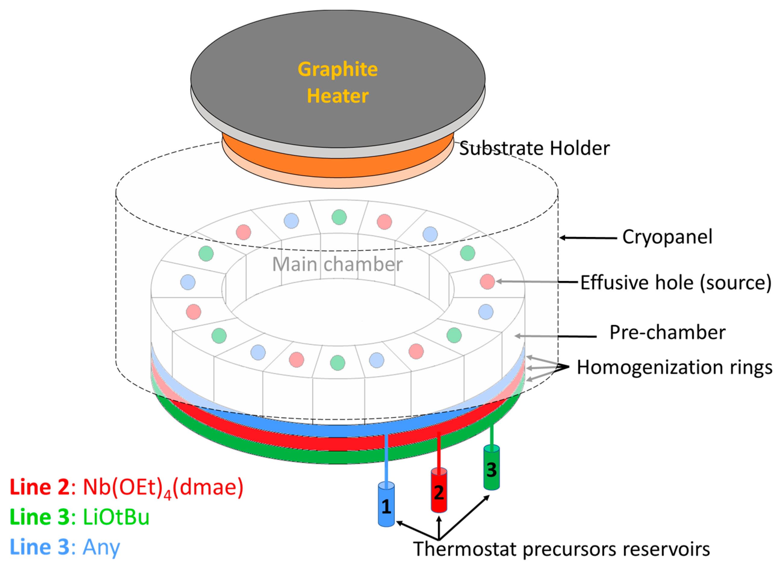
Lithium niobate films were deposited on a c-axis sapphire substrate by CBVD (chemical beam vapor deposition), also referred to as CBE (Chemical Beam Epitaxy), using Sybilla 200 equipment from ABCD Technology (see the principle in Figure 1). CBVD is a hybrid technique between MBE and CVD: its principle is based on chemical precursor flows under molecular vacuum conditions (meaning no gas-phase collisions, thus resulting in a line-of-sight deposition technique) [37,38,39,40]. The commercial precursors lithium tert-butoxide (hexameric in vapor phase [Li(OtBu)]6, CAS 1907-33-1) and niobium tetraethoxy dimethylaminoethoxide (Nb(OEt)4dmae, CAS 359847-15-7) are used as precursors. The precursor flows are evaluated theoretically from pre-chamber vapor pressures, which are adjusted via reservoir temperatures; details are described in our previous report [30]. In the present study, the Li precursor was positioned on line 1 with a pre-chamber vapor pressure of 6.7 × 10⁻³ mbar obtained with a reservoir temperature of 89.0 °C; and the Nb precursor was positioned on line 2 with a pre-chamber pressure of 29.0 × 10⁻³ mbar obtained with a reservoir temperature of 70.0 °C. Every source contained 3 holes that were 1.5 mm in diameter. Three opposite sources were used for each precursor, and the calculated Li/Nb precursor flow ratio at the best position was 1.44, (the principle of flow simulation was described in a previous paper [40]). This value is lower than the previously reported one by CBVD at 650 °C [30]. The substrate was heated with a graphite plate at 660 °C, resulting in an estimated substrate temperature of 400 °C evaluated by thermocouples positioned on the substrate holder. The deposition was carried out for three hours, and the simulation growth rate reached approximately 115 nm/h (slightly higher than at 650 °C for similar flow conditions). The deposition parameters are summarized in Table 1.
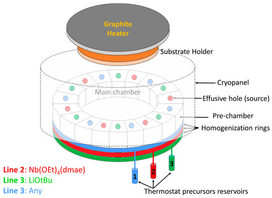
Figure 1.
Schematic of the CBVD/CBE Sybilla 200 system from ABCD Technology used in LiNbO3 thin film studies. Li precursor is located on line 1, and Nb is located on line 2. A thermostatic reservoir is employed to evaporate every precursor into a pre-chamber ring that is connected to 6 compartments with effusive holes on top. Through line-of-sight trajectories from the Knudsen holes, the precursor molecules reach the substrate and decompose due to the substrate heating.

Table 1.
Summary of deposition parameters of LiNbO3 thin film by CBVD.
3. Results and Discussion
3.1. Structure and Composition Properties
There is currently no quantitative method that is completely accurate in determining the Li/Nb ratio. Lithium is a very light element; its atomic mass is 6.941u and its atomic number is 3. Therefore, Ion Scattering Spectroscopy (ISS) and Energy-Dispersive X-ray Spectrometry (EDS) cannot detect lithium. The low intensity of the Li1s photoelectron line makes it difficult to provide accurate measurements by XPS [41,42].
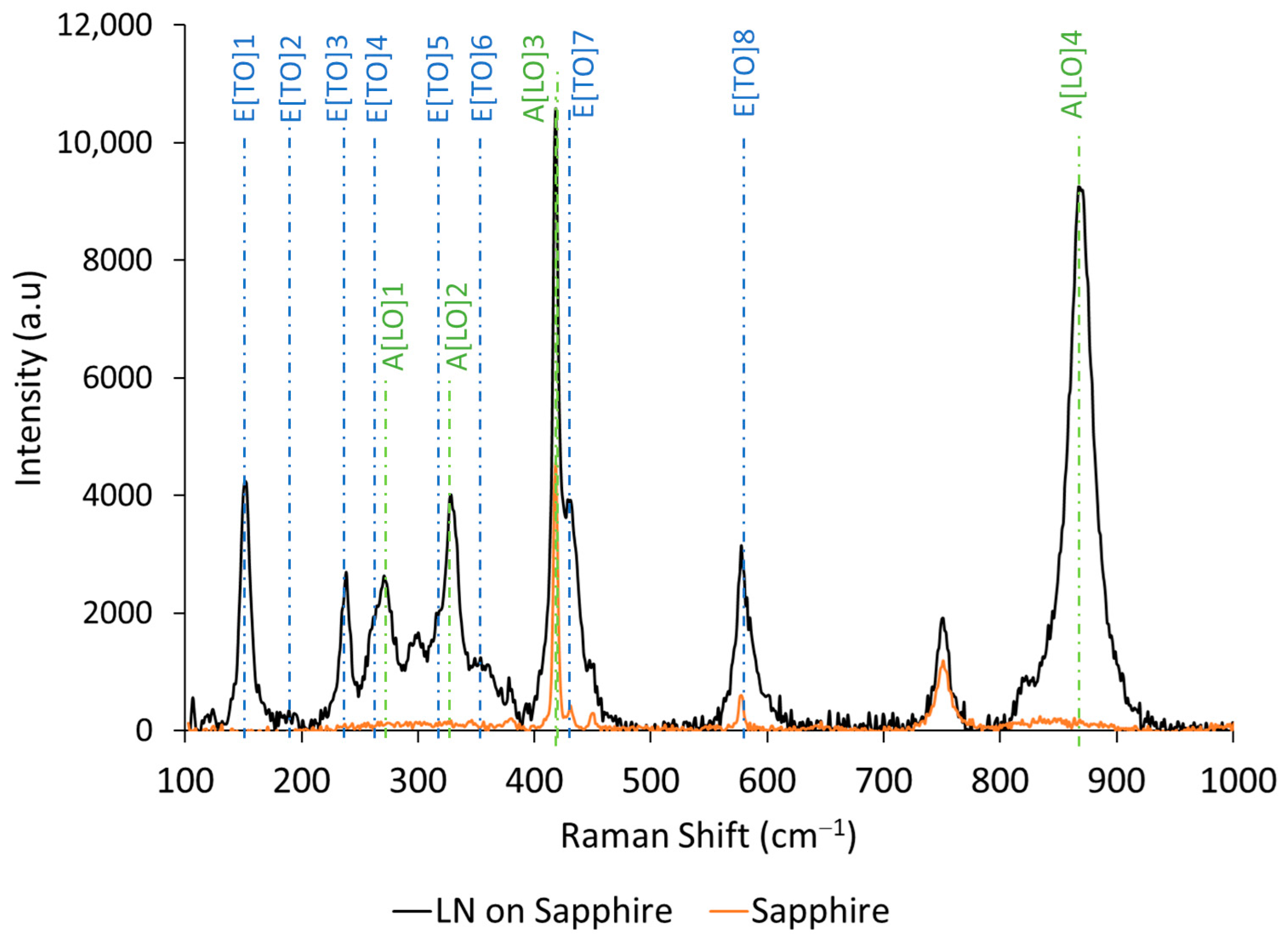
Raman spectroscopy is applied to estimate the chemical compositions of films. According to the difference in active scattering modes, the LiNbO3, LiNb3O8 and Li3NbO4 phases can be identified [43]. In this study, a Raman system was used at 633 nm laser wavelength with a lens magnification ×100. The Raman spectra of LiNbO3 film on sapphire and sapphire substrate spectra are presented in Figure 2. Peaks were measured at 152, 238, 270, 328, 428, 578 and 870 cm−1, which correspond to the expected modes of bulk LiNbO3 [44]. The vibrational modes of LiNb3O8 and Li3NbO4 could not be observed.
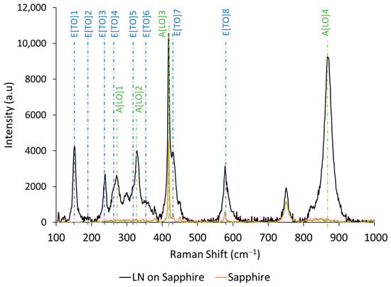
Figure 2.
Raman spectra of LiNbO3 thin films on sapphire (black line) and sapphire (orange line).
As reported by U. Schlarb et al. [45], the Li/Nb ratio can be estimated based on the relationship between the line width (Γ) of the peaks attributed to the E[TO]1 mode at 152 cm−1, the A[LO]4 at 870 cm−1 and the molar percentage of lithium content, which is described in Equations (1) and (2).
For 152 cm−1: [mol%]Li = 53.03 − 0.4739Γ (cm−1)
For 870 cm−1: [mol%]Li = 53.29 − 0.1837Γ (cm−1)
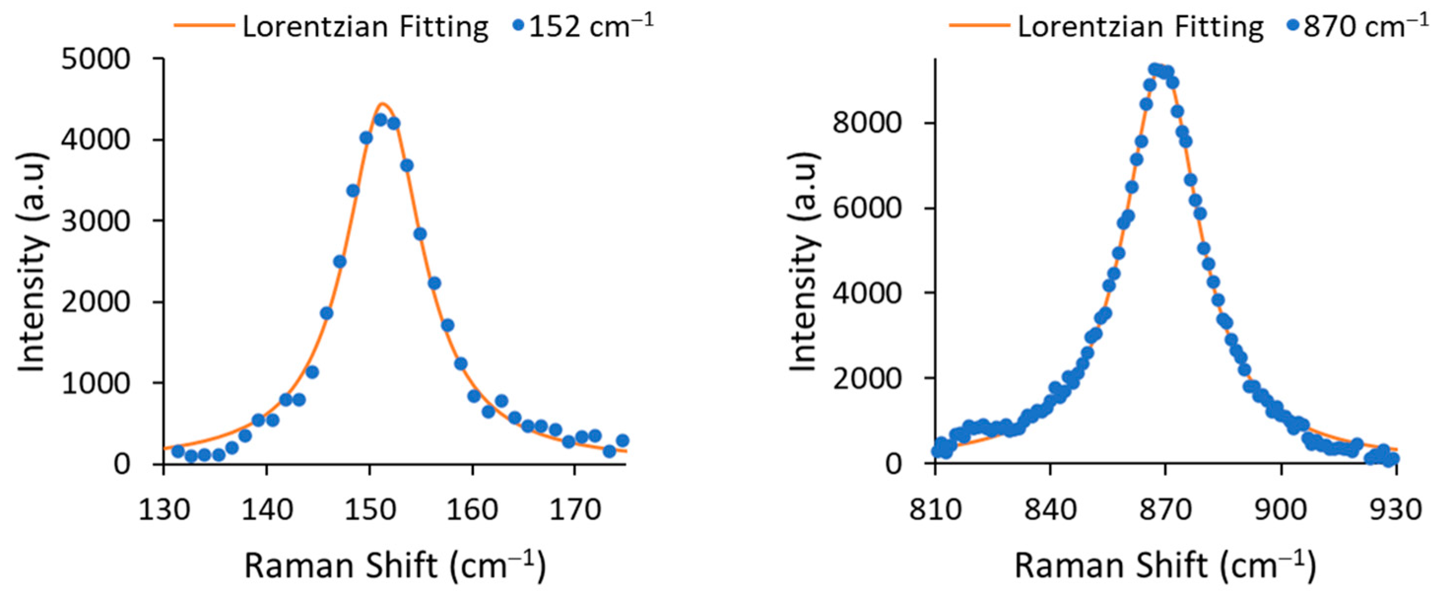
The line width Γ (or full width at half maximum, FWHM) was determined by fitting the experimental data with a Lorentzian function (see Figure 3). The extracted FWHMs were 9.19 cm−1 for 152 cm−1 mode and 24.01 cm−1 for 870 cm−1 mode, corresponding to Li concentrations [mole%] of 48.68% and 48.88%, respectively. According the results, the obtained material was congruent LiNbO3.
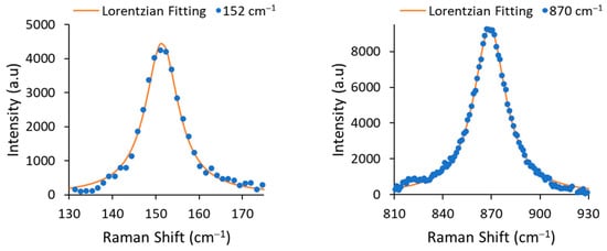
Figure 3.
A zoom-in on the 152 cm−1 and 870 cm−1 modes and their Lorentzian fitting curves.
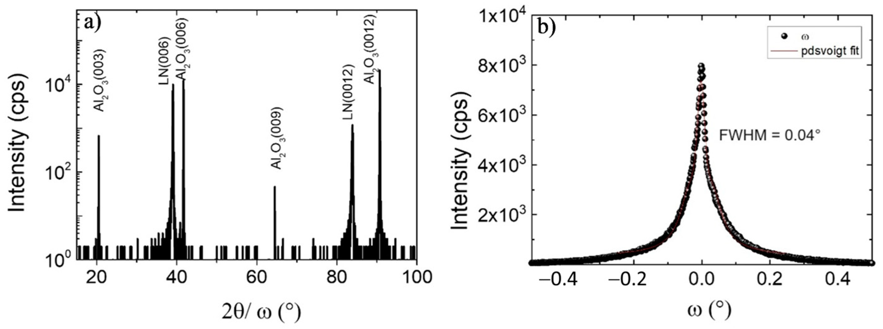
The crystal structure of LiNbO3 films was analyzed by high-resolution X-ray diffraction; the 2θ/ω pattern and rocking curve scan of LN (006) are illustrated in Figure 4. There were two peaks located at 38.94° and 83.92° which corresponded, respectively, to (006) and (0012) orientations of LiNbO3, which belonged to the same family of crystal planes. Combined with the Raman spectrum, this result strengthens the evidence for single-phase, c-axis oriented, LiNbO3 growth. The c lattice constant in this study equaled 13.833 Å; meanwhile, the c lattice constant of congruent LiNbO3 and stoichiometry LiNbO3 crystal were 13.864 Å and 13.856 Å, respectively [46], which shows some stresses are present in the film [47]. The crystalline quality of the layer was estimated by the FWHM of rocking curve scans on the LN (006) peak; the mosaicity was low at 0.04°. This value is comparable to those that were obtained at higher temperatures, such as 0.04° for MOCVD at 710 °C [31] and 0.03° for MBE at 1000 °C [18], and probably compete with 0.003° for LiNbO3 bulk [4]. The mosaicity of LiNbO3 films deposited by CBVD at 650 °C in a previous report was identical at 0.04° [30]. This result contributes to the ability to fabricate LiNbO3 thin film by CBVD at lower temperatures while maintaining the same crystal quality. M. Kadota et al. [28] fabricated a BAW resonator on LiNbO3 film deposited by CVD; the mosaicity of the LiNbO3 film was 0.4°, and the k2 equaled 5.8% at 2.9 GHz. Although this study showed higher mosaicity than bulk by one order of magnitude, it still holds promising potential for acoustic applications.
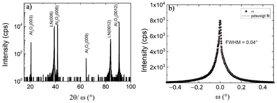
Figure 4.
(a) High-resolution X-ray diffraction diffractogram 2θ/ω scan of LiNbO3 from 15° to 100°, and (b) rocking curve on LN (006).
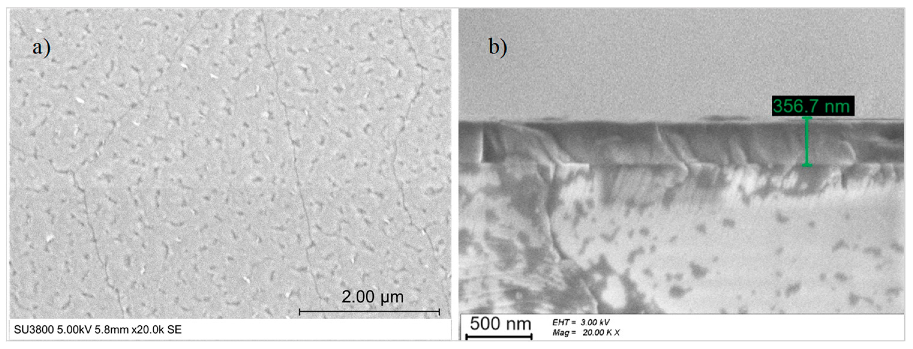
The surface morphology of LiNbO3 films was examined by SEM (see Figure 5a), but the resolution was too low to identify any grains. However, the film was cracked in random directions. The cracking of LiNbO3 film on c-plane sapphire is a well-known phenomenon [32], probably related to the different thermal expansion coefficients of Al2O3 and LiNbO3 perpendicular to the c-axis, 5.0 × 10⁻⁶ K−1 [48] and 14.1 × 10⁻⁶ K−1 [46], respectively. Besides that, the film thickness and the thermal processes (substrate temperature, heating and cooling step) affect the surface quality of LiNbO3 films. According to R. S. Feigelson [49], when the thickness of LiNbO3 deposited on c-plane sapphire is higher than 200 nm, cracks appear.
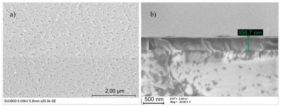
Figure 5.
(a) Top-view SEM image and (b) cross-section SEM image of LiNbO3 on sapphire c-plane.
The thickness measured in the SEM cross-section (see Figure 5b) was approx. 357 nm, and the growth rate equaled 119 nm/h.
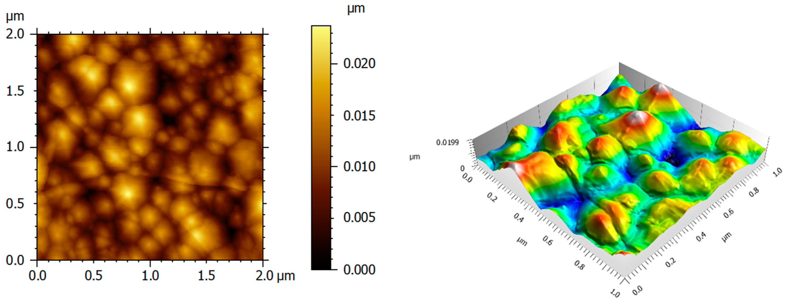
The surface topography of LiNbO3 films has been studied by AFM within the scanned area of 2 × 2 µm2 and 1 × 1 µm2, which is shown in Figure 6. The root mean square (rms) was obtained with a small value, equal to 2.0 nm.
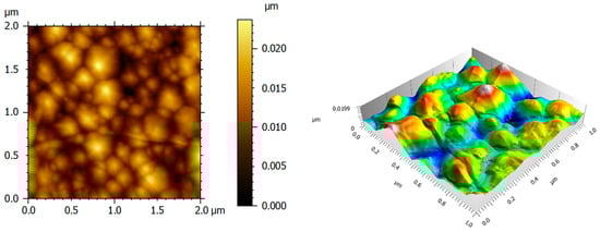
Figure 6.
Two-dimensional and three-dimensional AFM images of LiNbO3 thin on c-plane sapphire.
3.2. Optical Properties
The optical waveguide properties have been investigated using the prism coupling technique [50], which is also known as the m-line spectroscopy technique (system Metricon 2010 Ltd.). This technique provides the mapping of thickness, the refractive indices and the anisotropy (Δn = ne − no) of LiNbO3 films without destruction of the samples. In order to investigate the interaction of LiNbO3 films and light energy, different laser beam sources with wavelengths ranging from UV (450 nm) to near IR (1548 nm) were used. The laser beam with an incident angle (θ) was coupled into the layer via a right-angle rutile prism with an angle of 45° (code 4344.1 nm); then, the total reflected beam was collected by a photodetector. In this study, two waveguide modes were measured, the transverse electric waves (TE polarization) and the transverse magnetic waves (TM polarization). The returned indices nTE and nTM corresponded, respectively, to the ordinary refractive index (no) and extraordinary refractive index (ne). By identifying the reflectivity dips, referred to as propagation modes, the index and the thickness can be determined if at least two modes of the same polarization are observed. On the contrary, if there is only one mode of observation and the thickness is measured by other methods, the refractive index can still be extracted.
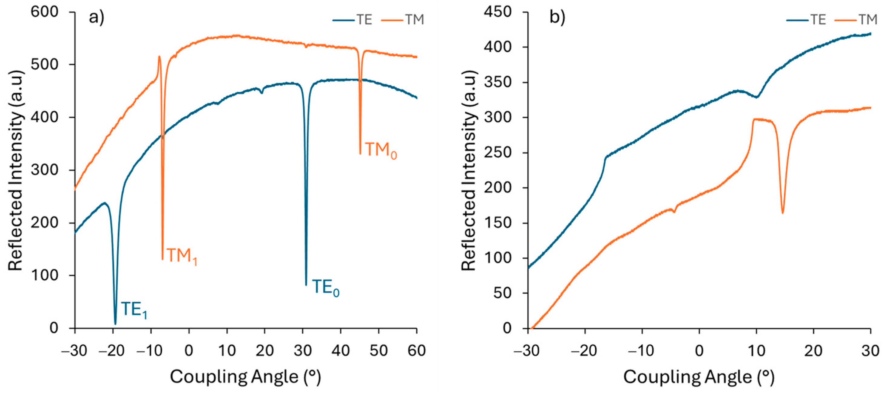
The TE- and TM-guided mode spectra at different laser wavelengths are illustrated in Figure 7. From 449.5 nm to 636.6 nm, two propagation modes are obtained in both TE and TM polarization. The sharp modes plotted for TE0 and TM0 were observed, indicating a smooth surface and a good film—substrate interface [51]. At a higher wavelength, there was only one mode due to the large difference between the thickness and the wavelength.
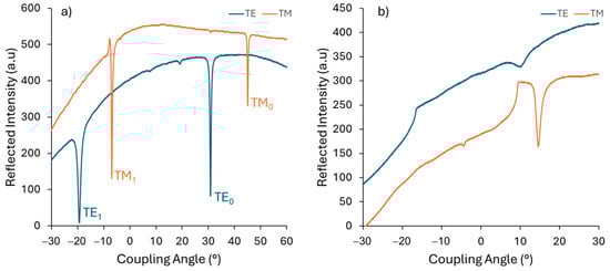
Figure 7.
Guided-mode spectrum obtained by measuring the reflected intensity versus the angle of incidence in TE and TM polarization at different light wavelengths: (a) 636.6 nm and (b) 1548.4 nm.
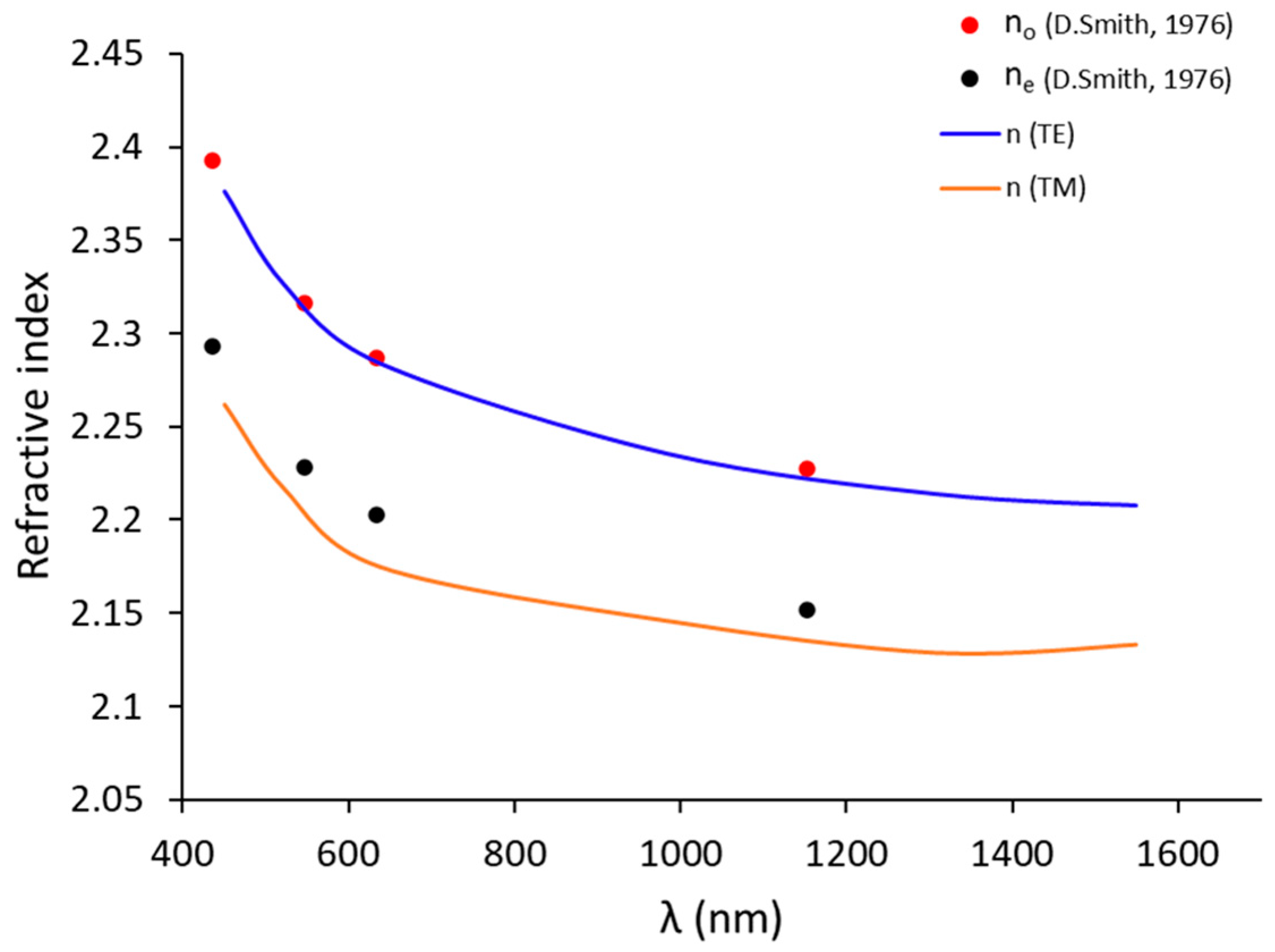
The refractive indices and film thickness were extracted by using the calculation procedure reported by Ulrich and Torge [52]. The mean thickness obtained at 449.5, 520.7 and 636.6 nm of wavelength was 357.7 ± 0.4 nm; this value was in good agreement with the thickness obtained by SEM cross-section (see Figure 5b). The refractive index dispersion as a function of the wavelength is summarized in Table 2 and Figure 8, with the values obtained matching with the literature [53]. The accuracy was 10−3 for the index.
Table 2.
The ordinary (nTE) and extraordinary (nTM) indices and the bi-refringence Δn of LiNbO3 film have been measured at different laser light wavelengths.
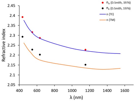
Figure 8.
The ordinary (nTE or no) and extraordinary (nTM or ne) indices (in blue line and orange line, respectively) in this study compared to the values no and ne indices (in red point and black point, respectively) [53] of bulk for congruent LiNbO3 (48.4% of Li).
In order to estimate the film composition, optical data could provide some information as reported in the literature. In 1993, Scharlb and Betzler [54] proposed a general Sellmeier equation for the ordinary and extraordinary optical index of LiNbO3 single crystals, valid in the wavelength range of 400–1200 nm and temperature range of 50–300 K and for Li-deficient LiNbO3 crystals in the range 47 to 50% Li.
The general equation is given as Equation (3), as follows, and the equation parameters are described in Ref [54], where the index e means extraordinary and the index o ordinary, with cLi in mol % Li2O, λ in nm, T in °C and T0 = 24.5 °C:
With:
Schlarb et al. [45] proposed a simple linear equation of the form to determine the composition cLi as a function of the measured bi-refringence of the LiNbO3 (difference between the ordinary and extraordinary index).
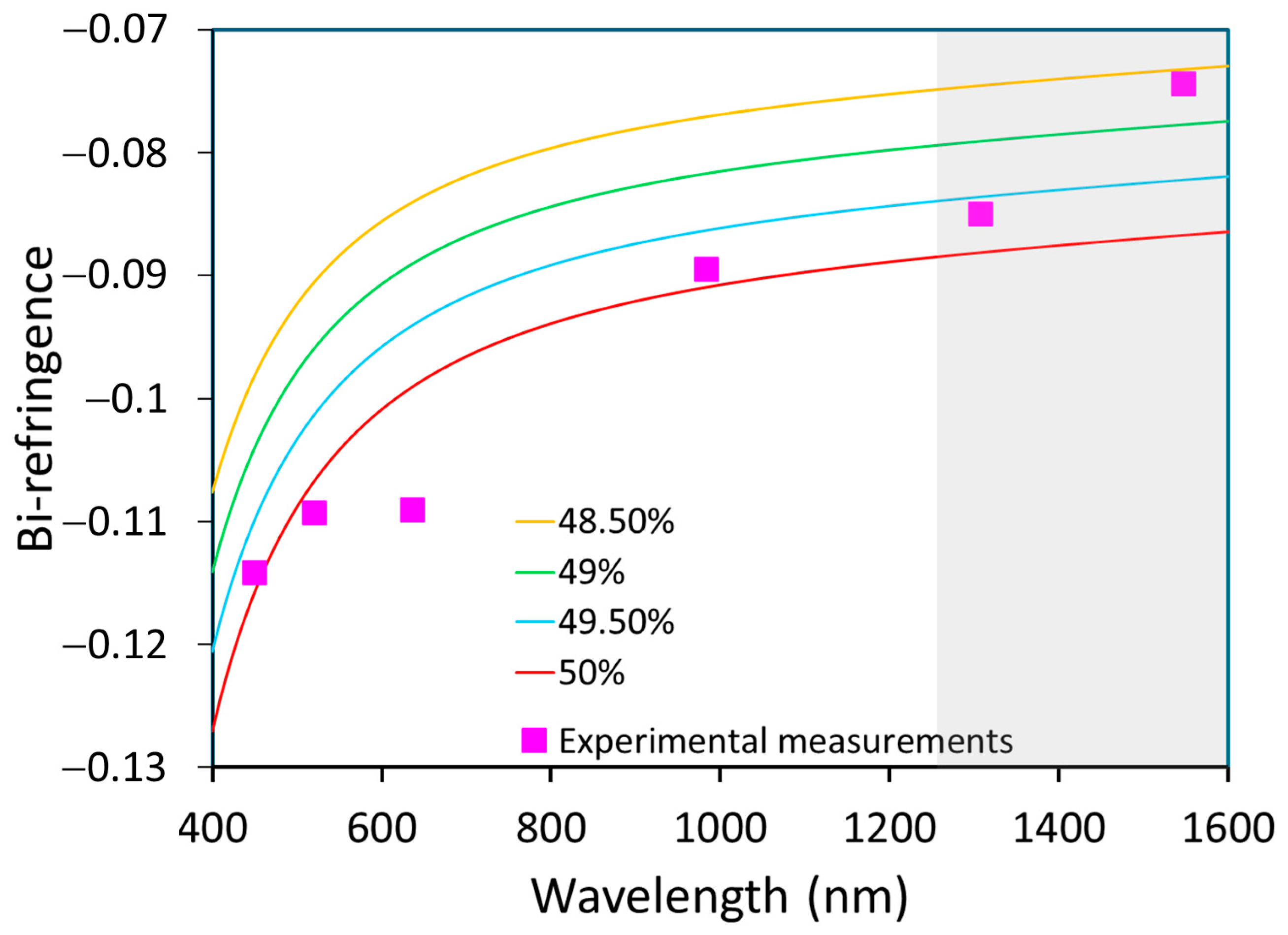
Based on Equations (3) and (4), values of a and b could be calculated at our measured wavelengths (it should be noted that we extrapolated values higher than 1200 nm). The estimated Li content is summarized in Table 3; the value obtained was near stoichiometry, slightly higher than the composition obtained by Raman. Figure 9 shows the variation in bi-refringence versus wavelength for different material compositions at 449.5, 520.7 and 983.9 nm, with the experimental data being close to the Schlarb model for 50% of Li content.
Table 3.
Estimation of the film composition (% of Li) with the Schlarb model from the experimental data of Table 2.
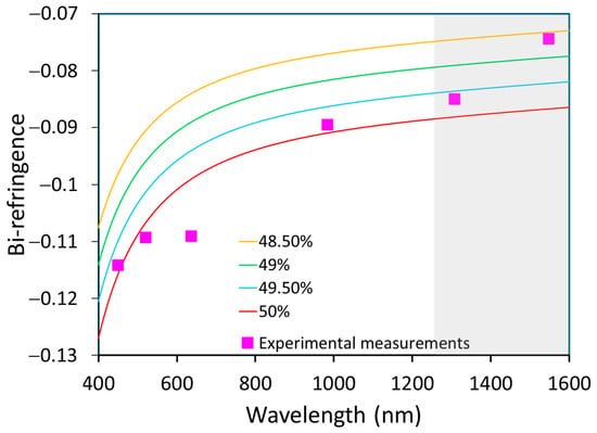
Figure 9.
Variation in bi-refringence as a function of wavelength for different material compositions (lines) and comparison to experimental points (pink). The gray region corresponds to an extrapolated range from literature equations.
4. Conclusions
Very high quality lithium niobate films were obtained on sapphire c-plane by the CBVD technique. HR-XRD patterns show a pure LiNbO3 phase and growth along the z direction, and the LiNbO3 (006) symmetric peak as measured by the rocking curve technique was 0.04° FWHM for 350 nm thick film. The Raman spectrum confirmed the results of HR-XRD; a composition of LiNbO3 was calculated by the line width (Γ) of the peaks at 152 cm−1 and 870 cm−1, giving a % of Li of 48.8 ± 0.15%. The refractive indices and bi-refringence were measured by the m-line spectroscopy technique, allowing another estimation of film composition and film thickness, which was not in agreement with values obtained from Raman and SEM.
The crystallinity of LiNbO3 film presented in this study for deposition at 400 °C matched those previously obtained for deposition at 650 °C by CBVD in our previous paper [30], only slightly reducing the Li/Nb precursor flow ratio to obtain the best films, and slightly increasing the growth rate. This demonstrates the ability to deposit LiNbO3 films by CBVD at lower temperatures while maintaining the film quality.
Author Contributions
Conceptualization, T.N.K.B.; methodology, G.B., E.W. and W.M.; characterization, T.N.K.B. and R.M.; validation, D.R., G.B. and E.H.D.; formal analysis, T.N.K.B. and E.W.; investigation, T.N.K.B. and R.M.; resources, T.N.K.B.; writing—original draft preparation, T.N.K.B.; writing—review and editing, D.R., G.B., E.H.D., R.B., B.M., K.D., W.M., E.W. and R.M.; visualization, T.N.K.B.; supervision, D.R., G.B. and E.H.D. All authors have read and agreed to the published version of the manuscript.
Funding
This research was funded by French Gorvenment, Agence Nationale de la Recherche (ANR) Plan de Relance 2020.
Institutional Review Board Statement
Not applicable.
Informed Consent Statement
Not applicable.
Data Availability Statement
The original contributions presented in the study are included in the article; further inquiries can be directed to the corresponding author.
Acknowledgments
The authors would like to express their sincere gratitude to Christian Grillet for his invaluable support in the characterization techniques conducted at the Institut des Nanotechnologies de Lyon (INL). His expertise and guidance greatly contributed to the success of this work. This project was funded by the French Government under the France Relance program, whose support is gratefully acknowledged.
Conflicts of Interest
The authors declare no conflicts of interest.
References
- Ballman, A.A. Growth of Piezoelectric and Ferroelectric Materials by the CzochraIski Technique. J. Am. Ceram. Soc. 1965, 48, 112–113. [Google Scholar] [CrossRef]
- Boes, A.; Chang, L.; Langrock, C.; Yu, M.; Zhang, M.; Lin, Q.; Lončar, M.; Fejer, M.; Bowers, J.; Mitchell, A. Lithium Niobate Photonics: Unlocking the Electromagnetic Spectrum. Science 2023, 379, eabj4396. [Google Scholar] [CrossRef] [PubMed]
- Levy, M.; Osgood, R.M.; Liu, R.; Cross, L.E.; Cargill, G.S.; Kumar, A.; Bakhru, H. Fabrication of Single-Crystal Lithium Niobate Films by Crystal Ion Slicing. Appl. Phys. Lett. 1998, 73, 2293–2295. [Google Scholar] [CrossRef]
- Zivasatienraj, B.; Brooks Tellekamp, M.; Alan Doolittle, W. Epitaxy of LiNbO3: Historical Challenges and Recent Success. Crystals 2021, 11, 397. [Google Scholar] [CrossRef]
- Takada, S.; Ohnishi, M.; Hayakawa, H.; Mikoshiba, N. Optical Waveguides of Single-Crystal LiNbO3 Film Deposited by Rf Sputtering. Appl. Phys. Lett. 1974, 24, 490–492. [Google Scholar] [CrossRef]
- Shimizu, M.; Furushima, Y.; Nishida, T.; Shiosaki, T. Preparation and Optical Waveguide Properties of LiNbO3 Thin Films by RF Magnetron Sputtering. Jpn. J. Appl. Phys. 1993, 32, 4111–4114. [Google Scholar] [CrossRef]
- Rost, T.A.; Lin, H.; Rabson, T.A.; Baumann, R.C.; Callahan, D.L. Deposition and Analysis of Lithium Niobate and Other Lithium Niobium Oxides by Rf Magnetron Sputtering. J. Appl. Phys. 1992, 72, 4336–4343. [Google Scholar] [CrossRef]
- Lansiaux, X.; Dogheche, E.; Remiens, D.; Guilloux-Viry, M.; Perrin, A.; Ruterana, P. LiNbO3 Thick Films Grown on Sapphire by Using a Multistep Sputtering Process. J. Appl. Phys. 2001, 90, 5274–5277. [Google Scholar] [CrossRef]
- Sauze, L.C.; Vaxelaire, N.; Rouchon, D.; Pierre, F.; Templier, R.; Remiens, D.; Rodriguez, G. Microstructural and Chemical Analysis of Polycrystalline LiNbO3 Films Obtained by Room-Temperature RF Sputtering after Various Annealing Durations. J. Vac. Sci. Technol. A 2020, 38, 043205. [Google Scholar] [CrossRef]
- Graça, M.P.F.; Prezas, P.R.; Costa, M.M.; Valente, M.A. Structural and Dielectric Characterization of LiNbO3 Nano-Size Powders Obtained by Pechini Method. J. Sol-Gel Sci. Technol. 2012, 64, 78–85. [Google Scholar] [CrossRef]
- Yoon, J.G.; Kim, K. Growth of Highly Textured LiNbO3 Thin Film on Si with MgO Buffer Layer through the Sol-Gel Process. Appl. Phys. Lett. 1995, 2523, 2523. [Google Scholar] [CrossRef]
- Nashimoto, K.; Cima, M.J. Epitaxial LiNbO3 Thin Films Prepared by a Sol-Gel Process. Mater. Lett. 1991, 10, 348–354. [Google Scholar] [CrossRef]
- Chen, Y.; Zhang, W.; Shu, Y.; Lou, C.; Kong, Y.; Huang, Z.; Xu, J.; Zhang, G. Determination of the Li/Nb Ratio in LiNbO3 Crystals Prepared by Vapor Transport Equilibration Method. Opt. Mater. 2003, 23, 295–298. [Google Scholar] [CrossRef]
- Han, H.; Cai, L.; Xiang, B.; Jiang, Y.; Hu, H. Lithium-Rich Vapor Transport Equilibration in Single-Crystal Lithium Niobate Thin Film at Low Temperature. Opt. Mater. Express 2015, 5, 2634. [Google Scholar] [CrossRef]
- Shih, W.C.; Sun, X.Y. Preparation of C-Axis Textured LiNbO3 Thin Films on SiO2/Si Substrates with a ZnO Buffer Layer by Pulsed Laser Deposition Process. Phys. B Condens. Matter 2010, 405, 1619–1623. [Google Scholar] [CrossRef]
- Shandilya, S.; Tomar, M.; Sreenivas, K.; Gupta, V. Structural and Interfacial Defects in C-Axis Oriented LiNbO3 Thin Films Grown by Pulsed Laser Deposition on Si Using Al: ZZnO Conducting Layer. J. Phys. D. Appl. Phys. 2009, 42, 095303. [Google Scholar] [CrossRef]
- Lee, G.H.; Yoshimoto, M.; Koinuma, H. Self-Assembled Island Formation of LiNbO3 by Pulsed Laser Deposition on α-Al2O3 Substrate. Appl. Surf. Sci. 1998, 127–129, 393–397. [Google Scholar] [CrossRef]
- Tellekamp, M.B.; Shank, J.C.; Goorsky, M.S.; Doolittle, W.A. Molecular Beam Epitaxy Growth of High Crystalline Quality LiNbO3. J. Electron. Mater. 2016, 45, 6292–6299. [Google Scholar] [CrossRef]
- Matsubara, K.; Niki, S.; Watanabe, M.; Fons, P.; Iwata, K.; Yamada, A. Growth of LiNbO3 Epitaxial Films by Oxygen Radical-Assisted Laser Molecular Beam Epitaxy. Appl. Phys. A 1999, 681, 679–681. [Google Scholar] [CrossRef]
- Tamada, H.; Yamada, A.; Saitoh, M. LiNbO3 Thin-Film Optical Waveguide Grown by Liquid Phase Epitaxy and Its Application to Second-Harmonic Generation. Appl. Phys. 1991, 70, 2536. [Google Scholar] [CrossRef]
- Yamada, A.; Tamada, H.; Saitoh, M. LiNbO3 Thin-Film Optical Waveguide Grown by Liquid Phase Epitaxy Using Li2O-B2O3 Flux. Appl. Phys. Lett. 1992, 61, 2848. [Google Scholar] [CrossRef]
- Miyazawa, S.; Fushimi, S.; Kondo, S. Optical Waveguide of LiNbO3 Thin Film Grown by Liquid Phase Epitaxy. Appl. Phys. Lett. 1975, 26, 8–10. [Google Scholar] [CrossRef]
- Wernberg, A.A.; Gysling, H.J.; Filo, A.J.; Blanton, T.N. Epitaxial Growth of Lithium Niobate Thin Films from a Single-Source Organometallic Precursor Using Metalorganic Chemical Vapor Deposition. Appl. Phys. Lett. 1993, 62, 946–948. [Google Scholar] [CrossRef]
- Ocón, J.A.; Murillo, J.G.; Miki-Yoshida, M.; Cardoza, M.N.; Contreras-López, O.E. Synthesis and Characterization of LiNbO3 Nanocrystals Prepared by the Aerosol Assisted Chemical Vapor Deposition Method. J. Cryst. Growth 2014, 408, 64–70. [Google Scholar] [CrossRef]
- Ocón-Arellanes, J.A.; Murillo-Ramírez, J.G.; Amézaga-Madrid, P.; Miki-Yoshida, M. Synthesis, Microstructural and Optical Characterization of LiNbO3 Thin Films Deposited by Aerosol Assisted Chemical Vapor Deposition. Acta Univ. 2014, 24, 21–26. [Google Scholar] [CrossRef]
- Sakashita, Y.; Segawa, H. Preparation and Characterization of LiNbO3 Thin Films Produced by Chemical-vapor Deposition. J. Appl. Phys. 1995, 77, 5995–5999. [Google Scholar] [CrossRef]
- Margueron, S.; Bartasyte, A.; Plausinaitiene, V.; Abrutis, A.; Boulet, P.; Kubilius, V.; Saltyte, Z. Effect of Deposition Conditions on the Stoichiometry and Structural Properties of LiNbO3 Thin Films Deposited by MOCVD. In Oxide-Based Materials and Devices IV; SPIE: San Francisco, CA, USA, 2013; Volume 8626. [Google Scholar] [CrossRef]
- Kadota, M.; Suzuki, Y.; Ito, Y. Properties of LiNbO3 Thin Film Deposited by Chemical Vapor Deposition and Frequency Characteristics of Film Bulk Acoustic Wave Resonator. Jpn. J. Appl. Phys. 2011, 50, 07HD10. [Google Scholar] [CrossRef]
- Dabirian, A.; Kuzminykh, Y.; Sandu, S.C.; Harada, S.; Wagner, E.; Brodard, P.; Benvenuti, G.; Rushworth, S.; Muralt, P.; Hoffmann, P. Combinatorial High-Vacuum Chemical Vapor Deposition of Textured Hafnium-Doped Lithium Niobate Thin Films on Sapphire. Cryst. Growth Des. 2011, 11, 203–209. [Google Scholar] [CrossRef]
- Pellegrino, A.L.; Wagner, E.; Lo Presti, F.; Maudez, W.; Kolb, S.; Rani, R.; Bernard, A.; Guy, S.; Gassenq, A.; Raevskaia, M.; et al. Efficient Optimization of High-Quality Epitaxial Lithium Niobate Thin Films by Chemical Beam Vapor Deposition: Impact of Cationic Stoichiometry. Adv. Mater. Interfaces 2023, 10, 2300535. [Google Scholar] [CrossRef]
- Lu, Z.; Hiskes, R.; DiCarolis, S.A.; Route, R.K.; Feigelson, R.S.; Leplingard, F.; Fouquet, J.E. Epitaxial LiNbO3 Thin Films on Sapphire Substrates Grown by Solid Source MOCVD. J. Mater. Res. 1994, 9, 2258–2263. [Google Scholar] [CrossRef]
- Bartasyte, A.; Plausinaitiene, V.; Abrutis, A.; Stanionyte, S.; Margueron, S.; Kubilius, V.; Boulet, P.; Huband, S.; Thomas, P.A. Thickness Dependent Stresses and Thermal Expansion of Epitaxial LiNbO3 Thin Films on C-Sapphire. Mater. Chem. Phys. 2015, 149, 622–631. [Google Scholar] [CrossRef]
- Sumets, M. Lithium Niobate-Based Heterostructures Synthesis, Properties and Electron Phenomena; IOP Publishing: Bristol, UK, 2018; ISBN 978-0-7503-1729-0. [Google Scholar]
- Qi, Y.; Li, Y. Integrated Lithium Niobate Photonics. Nanophotonics 2020, 9, 1287–1320. [Google Scholar] [CrossRef]
- Gorisse, M.; Bauder, R.; Timme, H.-J.; Friedrich, H.-P.; Dours, L.; Perreau, P.; Ravix, A.; Lefebvre, R.; Castellan, G.; Maeder-Pachurka, C.; et al. High Frequency LiNbO3 Bulk Wave Resonator. In Proceedings of the 2019 Joint Conference of the IEEE International Frequency Control Symposium and European Frequency and Time Forum (EFTF/IFC), Orlando, FL, USA, 14–18 April 2019; pp. 1–2. [Google Scholar]
- Plessky, V.; Yandrapalli, S.; Turner, P.J.; Villanueva, L.G.; Koskela, J.; Hammond, R.B. 5 GHz Laterally-Excited Bulk-Wave Resonators (XBARs) Based on Thin Platelets of Lithium Niobate. Electron. Lett. 2019, 55, 98–100. [Google Scholar] [CrossRef]
- Benvenuti, G.; Halary-Wagner, E.; Brioude, A.; Hoffmann, P. High Uniformity Deposition with Chemical Beams in High Vacuum. Thin Solid Films 2003, 427, 411–416. [Google Scholar] [CrossRef]
- Wagner, E.; Sandu, C.S.; Harada, S.; Pellodi, C.; Jobin, M.; Muralt, P.; Benvenuti, G. Geometry of Chemical Beam Vapor Deposition System for Efficient Combinatorial Investigations of Thin Oxide Films: Deposited Film Properties versus Precursor Flow Simulations. ACS Comb. Sci. 2016, 18, 154–161. [Google Scholar] [CrossRef]
- Dabirian, A.; Kuzminykh, Y.; Wagner, E.; Benvenuti, G.; Rushworth, S.; Hoffmann, P. Evaluation of Niobium Dimethylamino-Ethoxide for Chemical Vapour Deposition of Niobium Oxide Thin Films. Thin Solid Films 2014, 571, 94–101. [Google Scholar] [CrossRef]
- Wagner, E.; Maudez, W.; Bagdzevicius, S.; Sandu, S.C.; Benvenuti, G. Chemical Beam Vapour Deposition Technique with Sybilla Equipment: Review of Main Results in Its 20-Year Anniversary. In Oxide-Based Materials and Devices XII; Teherani, F.H., Look, D.C., Rogers, D.J., Eds.; SPIE: San Francisco, CA, USA, 2021; p. 64. [Google Scholar]
- Skryleva, E.A.; Kubasov, I.V.; Kiryukhantsev-Korneev, P.V.; Senatulin, B.R.; Zhukov, R.N.; Zakutailov, K.V.; Malinkovich, M.D.; Parkhomenko, Y.N. XPS Study of Li/Nb Ratio in LiNbO3 Crystals. Effect of Polarity and Mechanical Processing on LiNbO3 Surface Chemical Composition. Appl. Surf. Sci. 2016, 389, 387–394. [Google Scholar] [CrossRef]
- Skryleva, E.A.; Senatulin, B.R.; Kiselev, D.A.; Ilina, T.S.; Podgorny, D.A.; Parkhomenko, Y.N. Ar Gas Cluster Ion Beam Assisted XPS Study of LiNbO3 Z Cut Surface. Surf. Interfaces 2021, 26, 101428. [Google Scholar] [CrossRef]
- Bartasyte, A.; Plausinaitiene, V.; Abrutis, A.; Stanionyte, S.; Margueron, S.; Boulet, P.; Kobata, T.; Uesu, Y.; Gleize, J. Identification of LiNbO3, LiNb3O8 and Li3NbO4 Phases in Thin Films Synthesized with Different Deposition Techniques by Means of XRD and Raman Spectroscopy. J. Phys. Condens. Matter 2013, 25, 205901. [Google Scholar] [CrossRef]
- Galinetto, P.; Ballarini, D.; Grando, D.; Samoggia, G. Microstructural Modification of LiNbO3 Crystals Induced by Femtosecond Laser Irradiation. Appl. Surf. Sci. 2005, 248, 291–294. [Google Scholar] [CrossRef]
- Schlarb, U.; Klauer, S.; Wesselmann, M.; Betzler, K.; Wöhlecke, M. Determination of the Li/Nb Ratio in Lithium Niobate by Means of Birefringence and Raman Measurements. Appl. Phys. A Solids Surfaces 1993, 56, 311–315. [Google Scholar] [CrossRef]
- Nikogosyan, D.N. Basic Nonlinear Optical Crystals. In Nonlinear Optical Crystals: A Complete Survey; Springer: New York, NY, USA, 2005; pp. 5–74. ISBN 978-0-387-27151-4. [Google Scholar]
- Bartasyte, A.; Plausinaitiene, V.; Abrutis, A.; Murauskas, T.; Boulet, P.; Margueron, S.; Gleize, J.; Robert, S.; Kubilius, V.; Saltyte, Z. Residual Stresses and Clamped Thermal Expansion in LiNbO3 and LiTaO3 Thin Films. Appl. Phys. Lett. 2012, 101, 122902. [Google Scholar] [CrossRef]
- Aggarwal, R.L.; Ramdas, A.K. Physical Properties of Diamond and Sapphire, 1st ed.; CRC Press/Taylor & Francis Group: Boca Raton, FL, USA, 2019; ISBN 9780429283260. [Google Scholar]
- Feigelson, R.S. Epitaxial Growth of Lithium Niobate Thin Films by the Solid Source MOCVD Method. J. Cryst. Growth 1996, 166, 1–16. [Google Scholar] [CrossRef]
- Cardin, J.; Leduc, D. Determination of Refractive Index, Thickness, and the Optical Losses of Thin Films from Prism-Film Coupling Measurements. Appl. Opt. 2008, 47, 894–900. [Google Scholar] [CrossRef] [PubMed]
- Dogheche, E.; Lansiaux, X.; Remiens, D. M-Line Spectroscopy for Optical Analysis of Thick LiNbO3 Layers Grown on Sapphire Substrates by Radio-Frequency Multistep Sputtering. J. Appl. Phys. 2003, 93, 1165–1168. [Google Scholar] [CrossRef]
- Ulrich, R.; Torge, R. Measurement of Thin Film Parameters with a Prism Coupler. Appl. Opt. 1973, 12, 2901. [Google Scholar] [CrossRef]
- Smith, D.S.; Riccius, H.D.; Edwin, R.P. Refractive Indices of Lithium Niobate. Opt. Commun. 1976, 17, 332–335. [Google Scholar] [CrossRef]
- Schlarb, U.; Betzler, K. Refractive Indices of Lithium Niobate as a Function of Temperature, Wavelength, and Composition: A Generalized Fit. Phys. Rev. B 1993, 48, 15613–15620. [Google Scholar] [CrossRef]
Disclaimer/Publisher’s Note: The statements, opinions and data contained in all publications are solely those of the individual author(s) and contributor(s) and not of MDPI and/or the editor(s). MDPI and/or the editor(s) disclaim responsibility for any injury to people or property resulting from any ideas, methods, instructions or products referred to in the content. |
© 2024 by the authors. Licensee MDPI, Basel, Switzerland. This article is an open access article distributed under the terms and conditions of the Creative Commons Attribution (CC BY) license (https://creativecommons.org/licenses/by/4.0/).