Model Development for Threshold Voltage Stability Dependent on High Temperature Operations in Wide-Bandgap GaN-Based HEMT Power Devices

1
School of Optoelectronic Engineering and Instrumentation Science, Dalian University of Technology, Dalian 116024, China
2
Key Laboratory for Micro/Nano Technology and System of Liaoning Province, Dalian University of Technology, Dalian 116024, China
*
Author to whom correspondence should be addressed.
Micromachines 2018, 9(12), 658; https://doi.org/10.3390/mi9120658
Submission received: 23 November 2018
/
Revised: 23 November 2018
/
Accepted: 10 December 2018
/
Published: 14 December 2018
(This article belongs to the Special Issue Wide Bandgap Semiconductor Based Micro/Nano Devices)
Abstract
:Temperature-dependent threshold voltage (Vth) stability is a significant issue in the practical application of semi-conductor power devices, especially when they are undergoing a repeated high-temperature operation condition. The Vth analytical model and its stability are dependent on high-temperature operations in wide-bandgap gallium nitride (GaN)-based high electron mobility transistor (HEMT) devices that were investigated in this work. The temperature effects on the physical parameters—such as barrier height, conduction band, and polarization charge—were analysed to understand the mechanism of Vth stability. The Vth analytical model under high-temperature operation was then proposed and developed to study the measurement temperatures and repeated rounds dependent on Vth stability. The validity of the model was verified by comparing the theoretical calculation data with the experimental measurement and technology computer-aided design (TCAD) simulation results. This work provides an effective theoretical reference on the Vth stability of power devices in practical, high-temperature applications.
1. Introduction
Gallium nitride (GaN)-based high electron mobility transistors (HEMTs) have demonstrated a great potential in the fields of power electronics, mainly owing to their large semi-conductor bandgap (~3.4 eV), low intrinsic carrier concentration, and high-density two dimensional electron gas (2DEG) (>1013 cm−2), along with their high electron mobility (>2000 cm2∙V∙s−1) at the AlGaN/GaN heterojunction interface [1,2,3]. In comparison with Si or GaAs-based field-effect transistors (FETs), the wide-bandgap GaN-based devices have lower specific on-resistance and a faster ON/OFF switching speed. Therefore, they are well suited for high power switching applications in renewable energy systems, smart power grids, industrial motors, and the like. In particular, in the last decade, GaN-based HEMTs have attracted significant interest for high-frequency applications because the devices exhibit good noise properties comparable to GaAs-based HEMTs, but with the advantage of having a much higher input power robustness [4,5,6,7]. GaN-based HEMTs with a selected short gate length have overcome laterally diffused metal oxide semiconductor (LDMOS)-based transistors for the applications above the L-band owing to their higher frequency capabilities. Furthermore, GaN-based devices are also very promising when employed in various high-temperature environments, such as aerospace turbines and automotive internal combustion engines [8,9,10]. As a result of the considerable and worldwide attention given to the GaN techniques, they have achieved rapid and remarkable progress.
However, there are still several issues that need to be worked out for the practical application of GaN-based products [11,12]. An urgent task is to investigate the temperature-dependent performance stability, for instance, the device threshold voltage (Vth) stability [13]. To date, there has been much research on the temperature-dependent analytical model, focusing on investigating a device’s temperature-dependent output current–voltage characteristics and equivalent circuits. The temperature-dependent semi-conductor interface state and electron mobility have been extensively investigated [14,15,16,17]. The equivalent circuit modelling of GaN-based HEMTs as a function of ambient temperature has been accurately established, which is meaningful since the equivalent circuit is a very useful tool for circuit designers [18,19]. Besides, some work has studied the Vth variation according to the measurement temperature [20,21,22]. However, there is still a lack of sufficient research on the Vth analytical model and, in particular, on its stability when subjected to repeated high temperature operations, which might result in an unrecoverable impact on the material properties, for example the interface trap density.
This paper systematically investigates the Vth analytical model and the stability mechanism when subjected to the different measurement temperatures and repeated rounds in GaN-based HEMTs. Considering that a relatively large gate length of 2 µm was employed in the fabricated devices, the direct current (DC) characteristics are analysed in this work. The physical model was developed step-by-step by first building and analysing the Vth model in the conventional Schottky gate, with an emphasis on the influence of the physical parameters of the basic device on the Vth. The model was then analysed in the metal–insulator–semiconductor (MIS) gate structure, with an emphasis on the influence of the charged interface traps. A series of Vth values for the fabricated HEMTs were derived after repeating high-temperature measurements from room temperature to high-temperature for several rounds. The effects of the high temperature on the physical parameters, such as barrier height, conduction band, Fermi level, polarization charge, and interface traps were analysed to understand the Vth stability mechanism. Both the experimental measurement of the device and technology computer-aided design (TCAD) simulation work were carried out and the validity of the model was finally verified.
2. Physical Mechanism and Threshold Voltage (Vth) Analytical Model
Schottky contact is a basic element in power electronic devices. Therefore, physical modelling work starts with an investigation of the characteristics of simple Schottky-gate HEMT devices. The detailed study of effects of high-temperature on the Schottky-gate devices was carried out to understand the role of the basic physical parameters, such as barrier height, conduction band, Fermi level and polarization charges in the operation at high-temperature. Then, more complicated structures with the MIS gate were involved to analyse the effects of the interface traps beneath the gate, considering that the MIS gate structure has a much higher density of interface traps between the dielectric and AlGaN barrier layer than the Schottky gate. These charged traps could induce an instability of the Vth value, especially when the devices were operated under the high-temperature condition [23,24,25]. The physical mechanisms of the trap density variation with the different operation temperatures and sequences were discussed and the analytical model was proposed and developed.
2.1. Schottky-Gate AlGaN/GaN High Electron Mobility Transistors (HEMTs)
By taking into account the combined effects of the device’s physical parameters at different temperatures, such as Schottky barrier, polarization charges, energy band and doping-induced charges, the equation to generally describe the Vth of the Schottky-gate devices can be modified and expressed as below [26].
In the equation, is the contact barrier height between the gate metal and AlGaN barrier layer. is the conduction band offset at the AlGaN/GaN interface. is the energy difference between the intrinsic Fermi level and the conduction band edge of GaN bulk. is the net polarization charge at the AlGaN/GaN interface. Nd is the doping concentration in the AlGaN layer, and is the AlGaN permittivity. For simplicity, the AlGaN doping-induced effect on Vth can be ignored in the unintentionally doped AlGaN/GaN structure, due to its low intrinsic carrier concentration in the wide-bandgap semiconductor. Therefore, only the effects of the front four terms in Equation (1) were discussed here.
2.1.1. Schottky Barrier Height
The Schottky barrier height under zero bias can be determined by the expression [27]:
where and are the effective Schottky barrier height and ideality factor related to the applied electric field, respectively. They can be deduced from the experimental data using the expression . Here, IGS and VGS are the gate-to-source current and voltage, a is the gate contact area, and A* (= 28.4 A∙cm−2∙K−2) is the effective Richardson constant.
2.1.2. Conduction Band Offset
2.1.3. Fermi Energy
The Fermi energy level in GaN semiconductor can be defined by the empirical equation, as below [26].
where k1, k2, and k3 are the temperature-dependent parameters and ns is the sheet charge density.
2.1.4. Polarization Charge
High-density 2DEG will be formed at the AlGaN/GaN interface due to the existence of the large spontaneous and piezoelectric polarization induced electric field that can be determined by the elastic and piezoelectric constants of the materials in the c-axis direction. The sheet charge density induced by the net polarization will be deduced directly by the polarization expression from the published material parameters [28]. Although the net polarization-induced charge density is obviously changed depending on the Al composition and AlGaN barrier thickness, the pyroelectric coefficients that describe the changes in polarization depending on the temperature were found to be very small [30,31]. Chang et al. proved that the effect of pyroelectric coefficients on the channel current at high temperatures is negligible [3]. Therefore, the net polarization charge density was considered to be constant at a temperature less than 150 °C in this work.
2.2. Metal-Insulator-Semiconductor (MIS)-Gate AlGaN/GaN HEMTs
The Vth shift occurs more often in MIS-gate HEMTs than in Schottky-gate devices. The dominant reason is the existence of high-density traps at the dielectric/AlGaN interface near the gate. Although it is generally accepted that the Vth instability is induced by the combined effects of several trap species that are located in the GaN bulk or dielectric oxide or at the dielectric/AlGaN interface, the influence of the dielectric/AlGaN interface traps should be the most significant, given that it has the highest trap density (1012–1013 cm−2) and shortest distance to the 2DEG channel.
The band energy level of these traps plays an important role in determining the Vth values of the devices when they are operated at different high temperatures. Moreover, the amount of variation of these traps also affects the consistency of the Vth during repeated high-temperature operation. The trap amount will finally decrease and become stable after high-temperature measurements for several rounds. The repeated carrier injection and hopping among the traps due to thermal diffusion or the tunnelling process with the help of an electric field, are considered to be the main physical mechanisms that finally stabilize the trap energy level and amount after repeated high-temperature current–voltage (I-V) measurements. Therefore, the effects of the trap energy level and amount at the dielectric/AlGaN interface are included in this section to redefine the Vth in the MIS-gate AlGaN/GaN HEMTs. The Vth can be derived from the expressions below.
Here and are the thickness and dielectric constant of the gate oxide, respectively. and are the conduction band offsets at the AlGaN/GaN and dielectric/AlGaN interfaces, respectively. is the charged trap density at the dielectric/AlGaN interface which is varied with the measurement temperature and operation count at high temperature up to 150 °C. is the initial interface trap density. kt is the coefficient to describe the effect of the high-temperature measurement count on the trap amount and t is the repeated measurement rounds. is the variation value of the trap energy level at different measurement temperatures. NC, v, σn, and ED are the effective density of states in the conduction band, the thermal velocity of electrons, the capture cross section and the energetic location of the traps, respectively. EC − ED = 0.37 eV and v = 6 × 106 cm∙s−1 at AlGaN surface were used in the work [12].
The front six terms in Equation (8) describe the combined effects that originated from the basic physical parameters, i.e., the Schottky barrier, energy band, and polarization-induced charges on the Vth variation in the MIS-gate HEMTs, which are similar and consistent with the Schottky-gate case discussed earlier. The term in Equation (8) indicates an additional effect of the polarization-induced charges on the Vth by adding the gate oxide dielectric in the HEMTs. As mentioned, the effect was negligible since the variation of the polarization charge density with the temperature was small. The last term in Equation (8) related to the interface traps will play a key role in how the Vth changes with the measurement temperature and repeated rounds. Equation (9) is proposed to govern the amount variation of the charged interface traps, with increasing high temperature measurement rounds. Initially (t~0), NIT is equal to , corresponding to the case without any high-temperature operation. Then NIT decreased with the increasing measurement count t and finally the trap amount will be constant, and the Vth value will be stable from Equation (9). The coefficient kt is used to distinguish the effects of different measurement temperatures on the trap amount during the repeated high-temperature measurements. In Equation (10), the trap energy level is dependent on the temperature. The effective trap amount can be determined by the variation of the trap energy level with the increasing measurement temperature. In this work, the Shockley-Read-Hall (SRH) model was employed to describe the physical charge-trapping behaviour through the deep defect level in the gap. Several mathematical models were used to determine the temperature-dependent parameters, such as the material bandgap, Fermi level, polarization charge, carrier mobility and carrier lifetimes (or time constant) in the simulation work.
3. Experiments and Results
3.1. Fabrication and Measurement Process
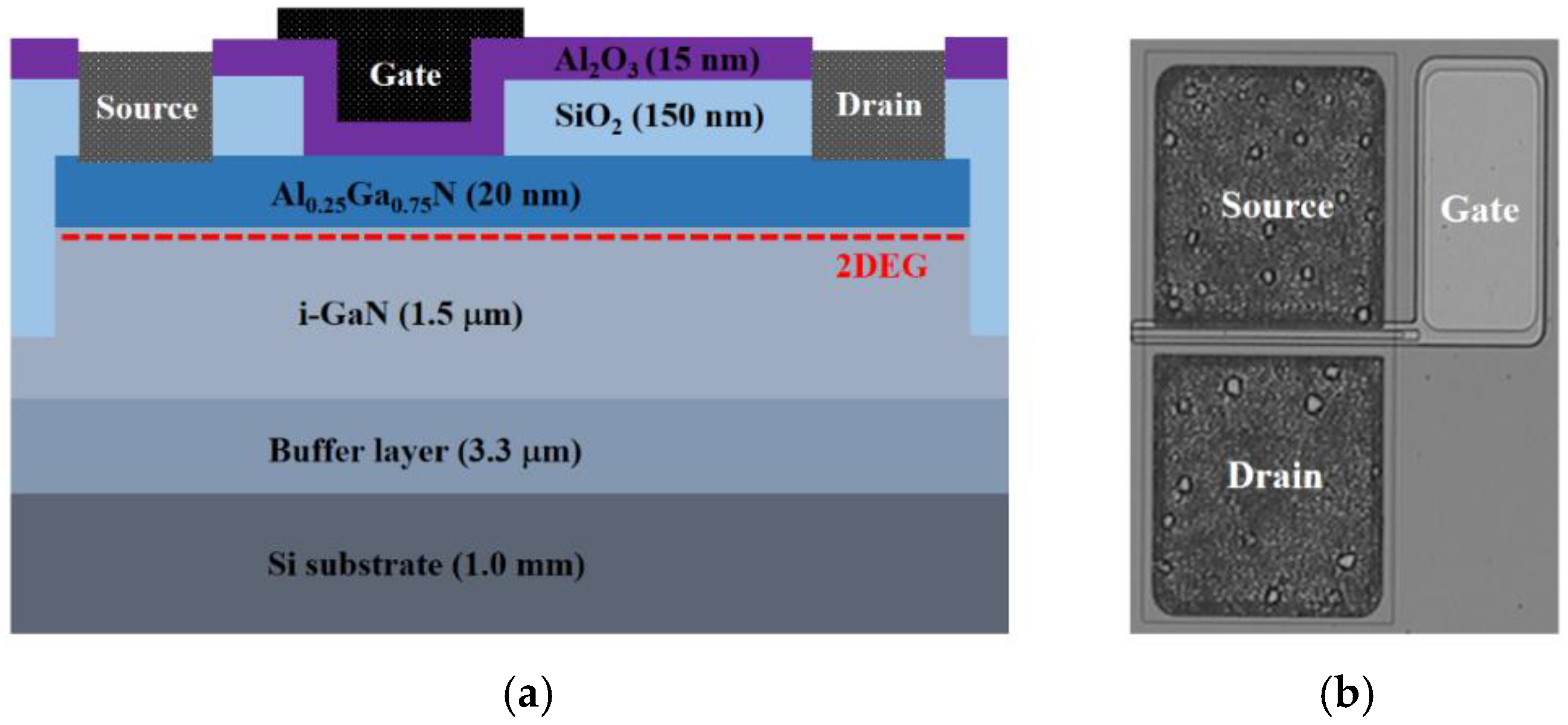
The schematic and optical microscopy image of the typical MIS-gate HEMTs are shown in Figure 1a,b, respectively. The specifics of the device structure are contained in Figure 1a. The fabrication work of the devices began with the mesa isolation by selectively etching the epitaxial layers with 300 nm depth. Ideal source and drain Ohmic contacts were achieved by depositing Ti/Al/Ni/Au (25 nm/125 nm/45 nm/55 nm) metal alloys using the E-beam system and annealing at 850 °C for 30 s in N2. SiO2 film with 150 nm thickness was deposited using a plasma-enhanced chemical vapour deposition (PECVD) system for surface passivation. Then the gate window with 2 µm length and 200 µm width was defined by photolithography, followed by the removal of the SiO2 film by wet etching. The Al2O3 gate dielectric layer with 15 nm thickness was deposited by the atomic layer deposition (ALD) system. Ni/Au metals were then deposited using the E-beam system for the gate electrode.
The I-V characteristics of the fabricated devices were measured at gradually increasing temperatures from 25 °C to 150 °C with a step of 25 °C using an Agilent B1505A semi-conductor device analyser (Agilent, Santa Clara, CA, USA). The measurement process was repeated for several rounds, and the testing platform was always cooled down naturally to room temperature before starting a new measurement round. Each measurement point was maintained at a setting temperature for 10 min in ambient air and then the drain current-gate voltage (Id-Vg) transfer curves were measured. The average measurement time for each I-V curve was around 2 s. The device-related physical parameters employed in the modelling and TCAD simulation processes were calibrated by benchmarking the device I-V characteristics with the measurement data. The typical parameter values are listed in Table 1 [12,32]. Verification was made by the simulation and laboratory measurement data to support the validity of the proposed model in the paper.
3.2. Model Verification and Discussion
3.2.1. Results for Schottky-Gate AlGaN/GaN HEMTs
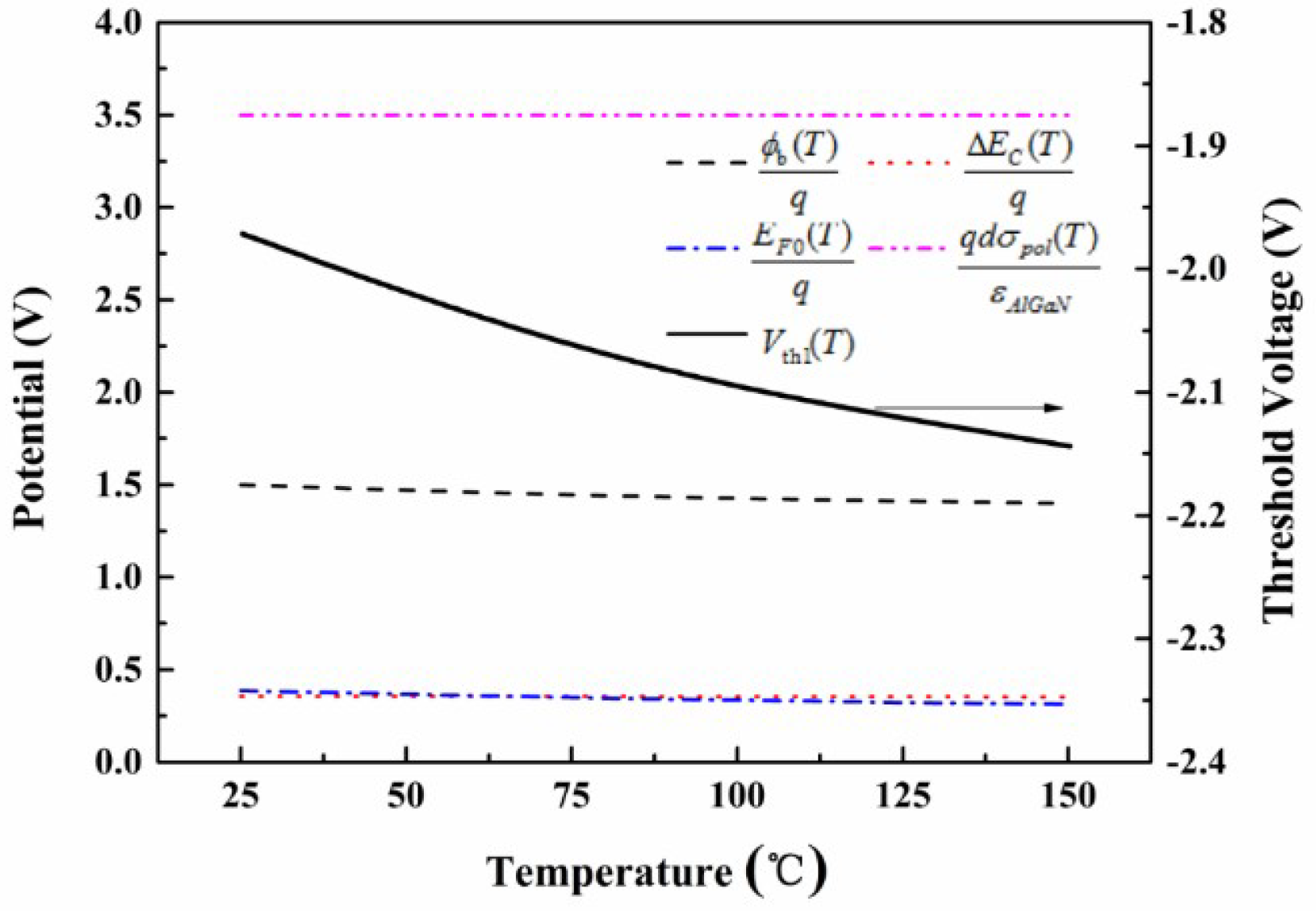
Figure 2 shows the detailed effects of the main physical parameters that varied with the temperature on the Vth stability. The Vth shifted slightly towards the negative direction as the temperature increased. The general effect on the Vth variation in the Schottky-gate HEMTs is displayed in Figure 2. The variation value of Vth was found to be around 0.15 V in the Schottky-gate devices when the temperature changed from 25 °C to 150 °C, which demonstrates that the Vth shift in Schottky-gate devices is relatively small.
3.2.2. Results for the MIS-Gate AlGaN/GaN HEMTs
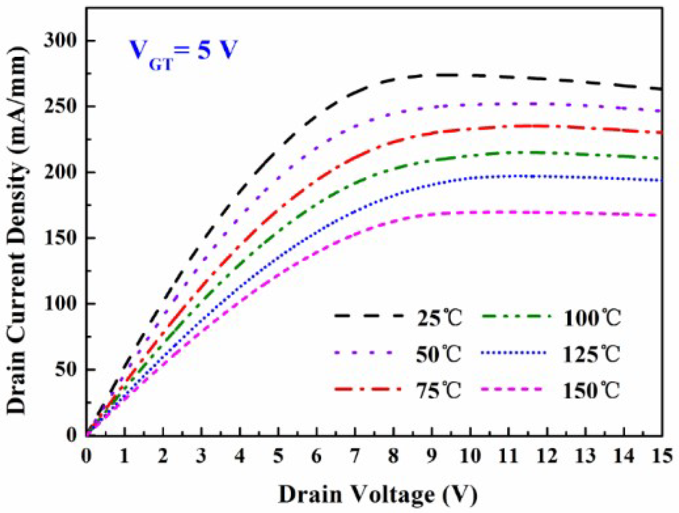
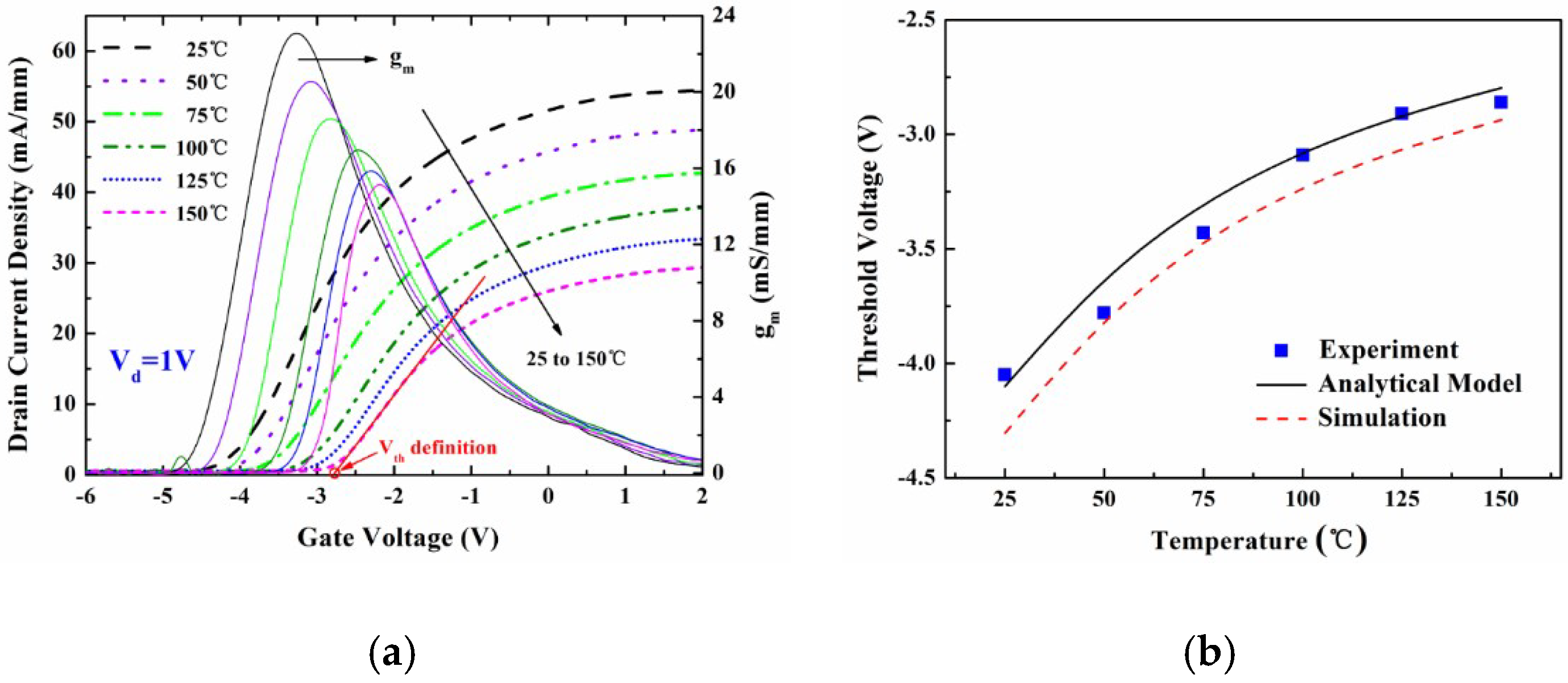
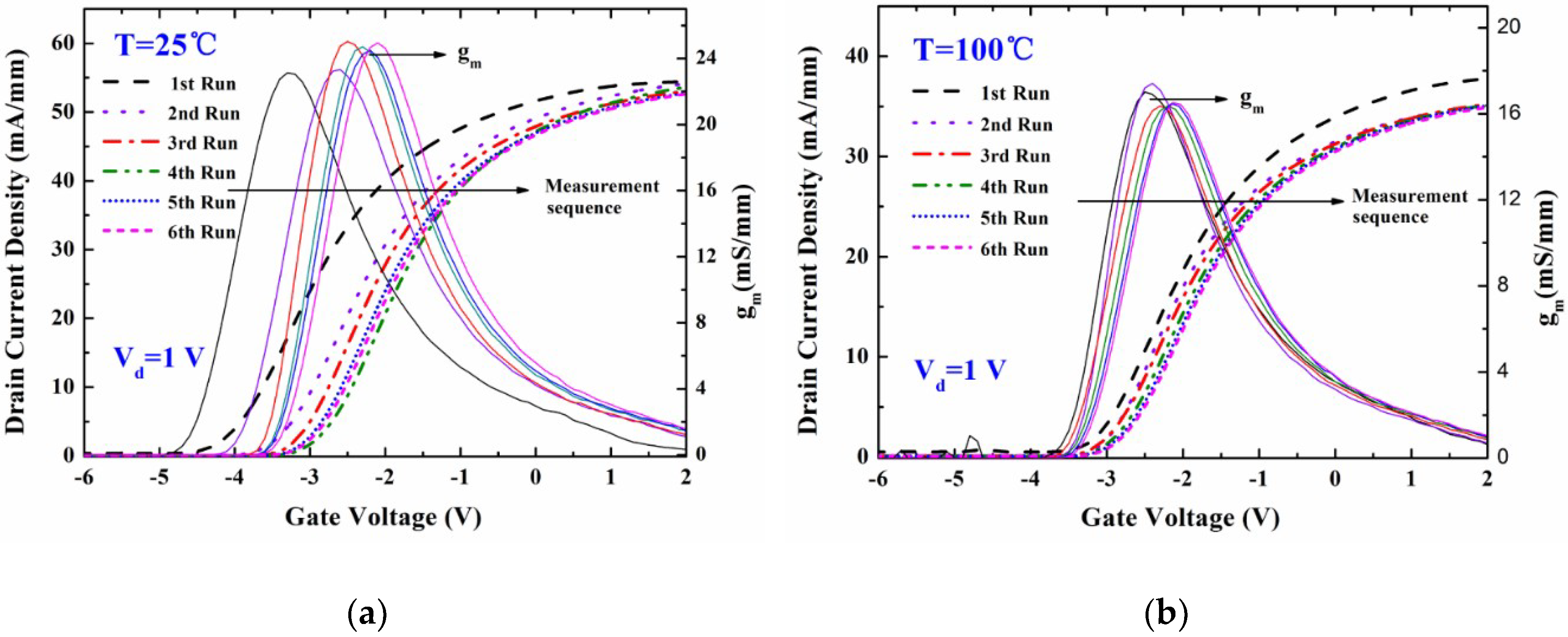
Figure 3 shows the measurement of the temperature-dependent DC output characteristics of the fabricated MIS-gate HEMTs. The drain current density decreased with the increasing temperature. This was mainly attributed to the degeneration of the electron mobility in the 2DEG channel induced by the thermal lattice vibration scattering. The source-to-drain channel conductance gds was found to be 52.3 mS/mm, 46.6 mS/mm, 39.8 mS/mm, 35.6 mS/mm, 30.4 mS/mm, and 27.5 mS/mm, respectively. Figure 4a shows the typical Id-Vg curves and gate transconductance gm characteristics of the fabricated MIS-gate, AlGaN/GaN HEMTs. The gm peak declined by 34.7% when the measurement temperature was up to 150 °C, which suggests a reduction of the device switching frequency.
The Vth values were determined by extrapolating the linear portion of the plot of the drain current density (Id) to the x axis (Vg). The intercept at the voltage axis was defined as the Vth in this paper. Vd = 1 V was used in the measurement process for the device transfer characteristics. An illustration of Vth definition is provided in Figure 4a. Figure 4b displays a trend of the Vth data variation with various temperatures. It was found that the measured Vth data shifted from −4.1 V to −2.7 V, towards more positive values with the increasing temperature. The big variance likely mainly originated from the combined effects of the change of interface trap number and the shift of the trap energy level during the process of the temperature increasing. More electrons may be captured by high-density ionized donor-like traps at the Al2O3/AlGaN interface beneath the gate at high temperatures. Thus, the number of the interface positive charges decreased, which resulted in the shift of the Vth. Equation (10) was employed to clearly describe the relationship between the trap density and the operation temperature. Both the calculation results based on the proposed analytical model and the simulation work agree well with the experimental data, which supports the validity of the physical model.
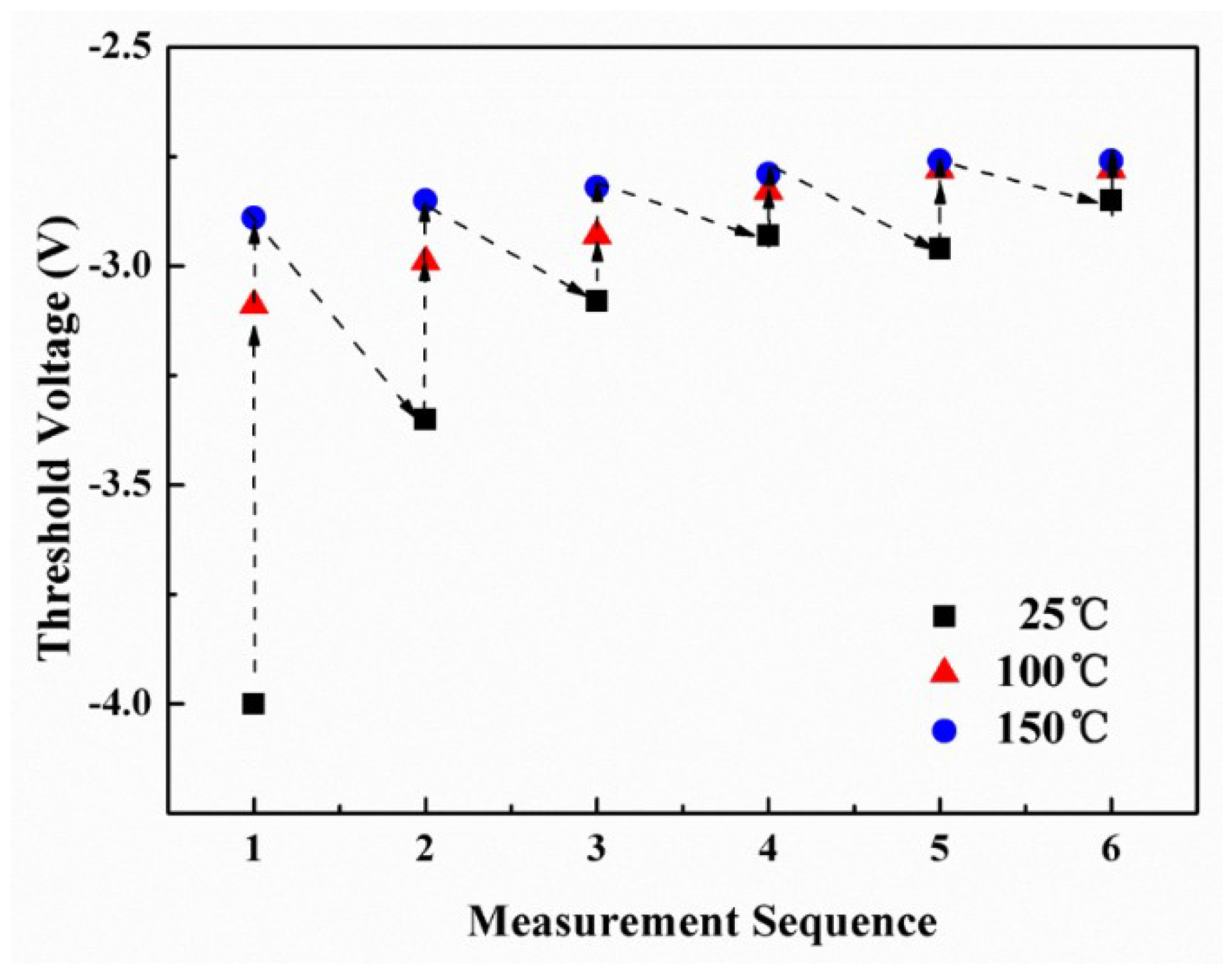
Figure 5 shows the repeated measurement-dependence of the DC output characteristics of the fabricated MIS-gate HEMTs, which demonstrates that the drain current remained almost unchanged even after several rounds of I-V measurements. Figure 6 shows the typical Id-Vg curves and gm characteristics of the fabricated MIS-HEMTs, dependent on the repeated measurement rounds. The gm peak changed slightly after several measurement rounds and the variation was less than 7.8%. Figure 7 displays the Vth values and the measurement flow. The data were measured at gradually increased temperatures from 25 °C to 150 °C and then the sample was cooled down naturally to room temperature before starting a new measurement round. The measurement process was repeated for several rounds until the Vth value was stable. Thus, the repeated measurement dependence of the Vth was achieved, as shown in Figure 7. A big variance around 1.1 V was found at the beginning, while the Vth value was kept nearly constant and only a small change of 0.1 V was found after several rounds of high-temperature measurements. This indicates that most ionized donor-like traps capture the free electrons and hence the number of charged traps is finally close to constant.
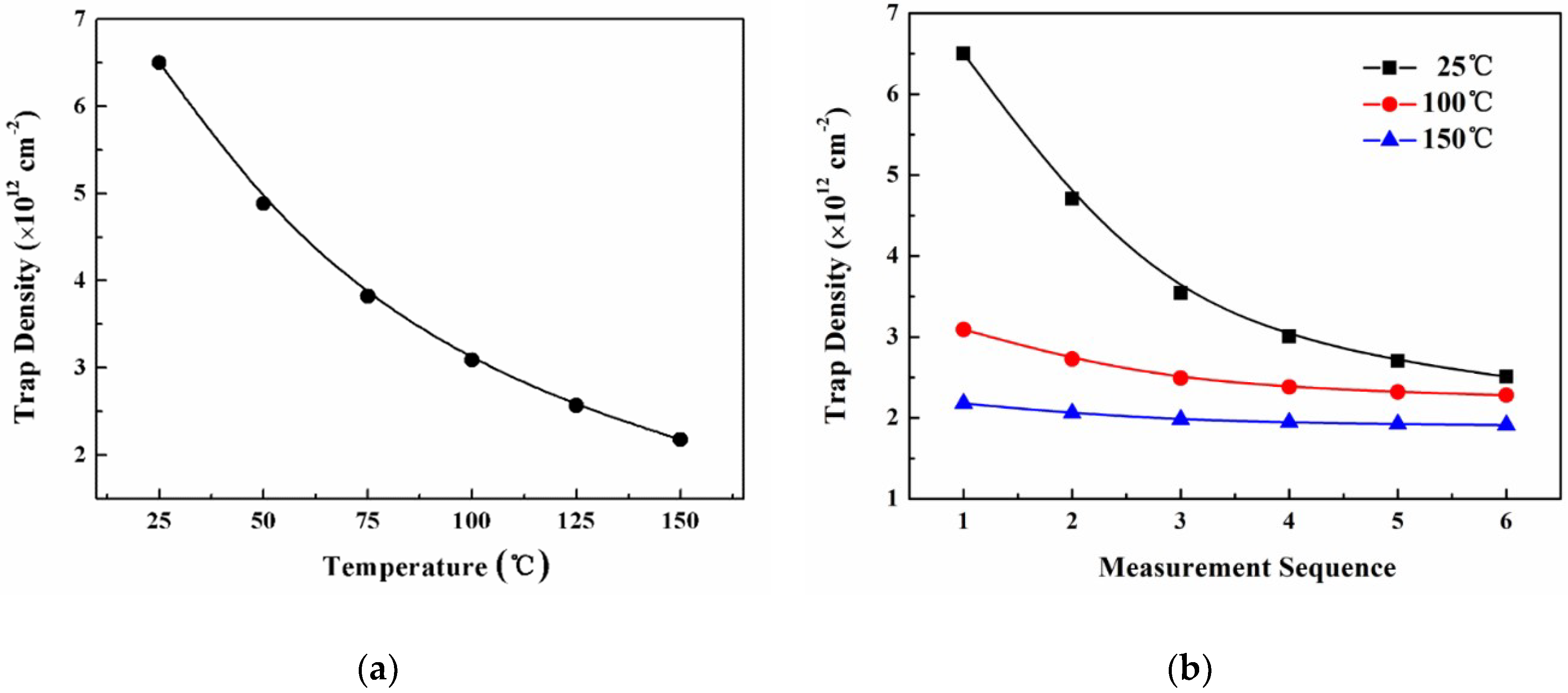
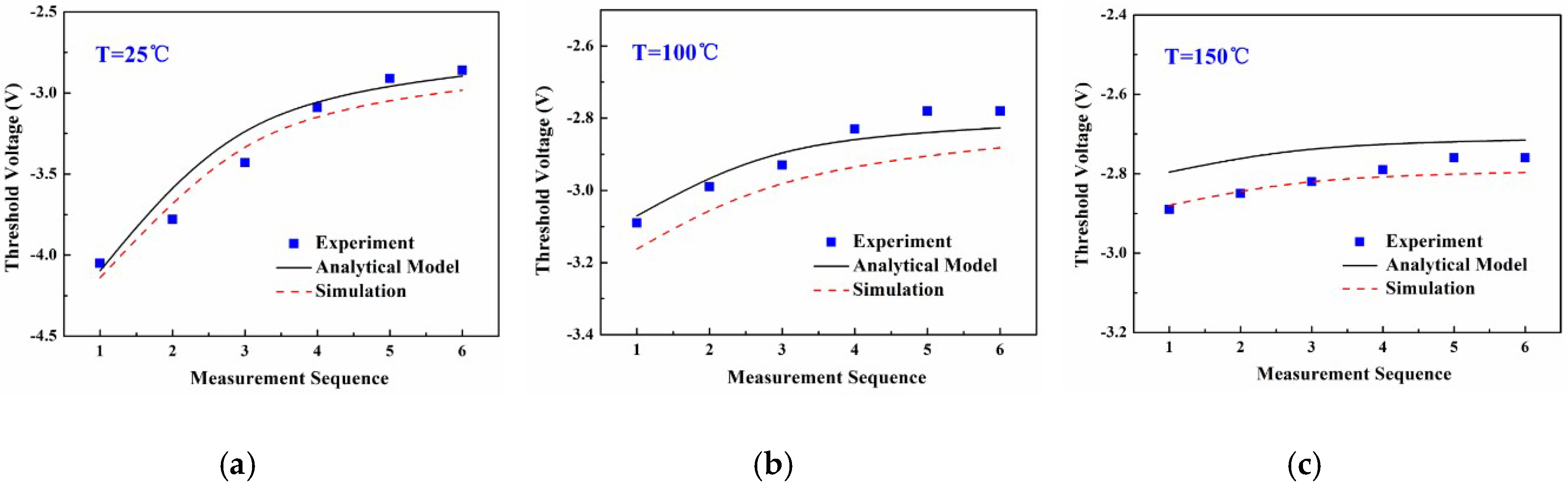
Figure 8 shows the employed trap density data at the Al2O3/AlGaN interface in the analytical model and TCAD simulation, which are dependent on the measurement temperature and sequence. The amount of variation of these charged traps greatly affected the consistency of the Vth during the repeated high-temperature operations. The charged trap amount was assumed to decrease with the increasing measurement rounds and finally became stable in the proposed physical model. The repeated carrier injection and hopping among the traps by the thermal diffusion and/or tunnelling process in the measurements, were considered to be the main physical mechanism responsible for the amount of variation of the charged traps. This process might repair some defects to some extent, and finally stabilizes the charged trap number after repeated high-temperature I-V measurements. Future work should explore whether the applied low electric field at high temperatures helps to repair the interface defects around the gate. Equation (9) in the manuscript was employed to govern the amount of variation of the traps with the increasing high-temperature measurement rounds. Figure 9 displays the Vth values that changed with the measurement sequence based on the experimental measurement, analytical model, and TCAD simulation work. The results were basically consistent and the average mismatch for the Vth value was kept within 5%, which again supports the validity of the physical model.
4. Conclusions
GaN-based HEMT devices were fabricated and measured to investigate the effects of the operation temperature and repeated rounds on the Vth stability. The Vth analytical model was proposed and developed to study the mechanism of the Vth variations in the repeated high-temperature operations. The combined effects of the amount of change of the interface charged traps and the shift of the trap energy level were considered to be the main reason for the Vth shift. The validity of the proposed analytical model was verified by experimental measurement and TCAD simulation results. The work can assist the engineers find a better understanding of the Vth stability of power devices in practical high-temperature applications.
Author Contributions
Data curation, F.L.; Investigation, Z.S.; Software, Y.C.; Writing—review and editing, H.H.
Funding
This research was funded by the National Science Foundation of China (grant number 51607022), the Fundamental Research Funds for the Central Universities (grant number DUT17LK13), the Major University Science Research Project of Anhui Province (grant number KJ2016SD42), the Open Project Program of Key Lab of Semiconductor Materials Science (grant number KLSMS-1610) and the Open Project Program of Key Laboratory of Nanodevices and Applications (grant number 18JG02) from Chinese Academy of Sciences.
Acknowledgments
The authors are also grateful to the National University of Singapore and Yung C. Liang for his time and help.
Conflicts of Interest
The authors declare no conflict of interest.
References
- Chen, C.; Liu, X.Z.; Tian, B.L.; Shu, P.; Chen, Y.F.; Zhang, W.L.; Jiang, H.C.; Li, Y.R. Fabrication of Enhancement-Mode AlGaN/GaN MISHEMTs by Using Fluorinated Al2O3 as Gate Dielectrics. IEEE Electron Device Lett. 2011, 32, 1373–1375. [Google Scholar] [CrossRef]
- Zhang, Y.H.; Sun, M.; Joglekar, S.J.; Fujishima, T.; Palacios, T. Threshold voltage control by gate oxide thickness in fluorinated GaN metal-oxide-semiconductor high-electron-mobility transistors. Appl. Phys. Lett. 2013, 103, 033524. [Google Scholar] [CrossRef] [Green Version]
- Chang, Y.; Tong, K.Y.; Surya, C. Numerical simulation of current–voltage characteristics of AlGaN/GaN HEMTs at high temperatures. Semicond. Sci. Technol. 2005, 20, 188. [Google Scholar] [CrossRef]
- Campbell, C.F.; Balistreri, A.; Kao, M.Y.; Dumka, D.C.; Hitt, J. GaN Takes the Lead. IEEE Microw. Mag. 2012, 13, 44–53. [Google Scholar] [CrossRef]
- Crupi, G.; Vadala, V.; Colantonio, P.; Cipriani, E.; Caddemi, A.; Vannini, G.; Schreurs, D.M.M.P. Empowering GaN HEMT models: The gateway for power amplifier design. Int. J. Numer. Model. Electron. Netw. Devices Fields 2017, 30, e2125. [Google Scholar] [CrossRef]
- Quaglia, R.; Camarchia, V.; Pirola, M.; Ghione, G. GaN Monolithic Power Amplifiers for Microwave Backhaul Applications. Electronics 2016, 5, 25. [Google Scholar] [CrossRef]
- Nalli, A.; Raffo, A.; Crupi, G.; D’Angelo, S.; Resca, D.; Scappaviva, F.; Salvo, G.; Caddemi, A.; Vannini, G. GaN HEMT Noise Model Based on Electromagnetic Simulations. IEEE Trans. Microw. Theory 2015, 63, 2498–2508. [Google Scholar] [CrossRef]
- Gurpinar, E.; Castellazzi, A. Tradeoff Study of Heat Sink and Output Filter Volume in a GaN HEMT Based Single-Phase Inverter. IEEE Trans. Power Electr. 2018, 33, 5226–5239. [Google Scholar] [CrossRef] [Green Version]
- Li, J.; Mao, S.; Xu, Y.; Zhao, X.; Wang, W.; Guo, F.; Zhang, Q.; Wu, Y.; Zhang, B.; Chen, T.; et al. An Improved Large Signal Model for 0.1 μm AlGaN/GaN High Electron Mobility Transistors (HEMTs) Process and Its Applications in Practical Monolithic Microwave Integrated Circuit (MMIC) Design in W band. Micromachines 2018, 9, 396. [Google Scholar] [CrossRef] [PubMed]
- Bae, K.T.; Lee, I.J.; Kang, B.; Sim, S.; Jeon, L.; Kim, D.W. X-Band GaN Power Amplifier MMIC with a Third Harmonic-Tuned Circuit. Electronics 2017, 6, 103. [Google Scholar] [CrossRef]
- Meneghini, M.; Rossetto, I.; Rizzato, V.; Stoffels, S.; Van Hove, M.; Posthuma, N.; Wu, T.L.; Marcon, D.; Decoutere, S.; Meneghesso, G.; et al. Gate Stability of GaN-Based HEMTs with P-Type Gate. Electronics 2016, 5, 14. [Google Scholar] [CrossRef]
- Huang, H.L.; Sun, Z.H.; Cao, Y.Q.; Li, F.Y.; Zhang, F.; Wen, Z.X.; Zhang, Z.F.; Liang, Y.C.; Hu, L.Z. Investigation of surface traps-induced current collapse phenomenon in AlGaN/GaN high electron mobility transistors with schottky gate structures. J. Phys. D Appl. Phys. 2018, 51, 345102. [Google Scholar] [CrossRef]
- He, J.; Hua, M.; Zhang, Z.; Chen, K.J. Performance and Vth Stability in E-Mode GaN Fully Recessed MIS-FETs and Partially Recessed MIS-HEMTs with LPCVD-SiNx/PECVD-SiNx Gate Dielectric Stack. IEEE Trans. Electron Devices 2018, 65, 3185–3191. [Google Scholar] [CrossRef]
- Jogai, B. Influence of surface states on the two-dimensional electron gas in AlGaN/GaN heterojunction field-effect transistors. J. Appl. Phys. 2003, 93, 1631–1635. [Google Scholar] [CrossRef]
- Horio, K.; Yonemoto, K.; Takayanagi, H.; Nakano, H. Physics-based simulation of buffer-trapping effects on slow current transients and current collapse in GaN field effect transistors. J. Appl. Phys. 2005, 98, 124502. [Google Scholar] [CrossRef]
- Lin, Y.S.; Wu, J.Y.; Chan, C.Y.; Hsu, S.S.H.; Huang, C.F.; Lee, T.C. Square-Gate AlGaN/GaN HEMTs With Improved Trap-Related Characteristics. IEEE Trans. Electron Devices 2009, 56, 3207–3211. [Google Scholar] [CrossRef]
- Brannick, A.; Zakhleniuk, N.A.; Ridley, B.K.; Shealy, J.R.; Schaff, W.J.; Eastman, L.F. Influence of Field Plate on the Transient Operation of the AlGaN/GaN HEMT. IEEE Electron Device Lett. 2009, 30, 436–438. [Google Scholar] [CrossRef]
- Wang, C.S.; Xu, Y.H.; Yu, X.M.; Ren, C.J.; Wang, Z.S.; Lu, H.Y.; Chen, T.S.; Zhang, B.; Xu, R.M. An Electrothermal Model for Empirical Large-Signal Modeling of AlGaN/GaN HEMTs Including Self-Heating and Ambient Temperature Effects. IEEE Trans. Microw. Theory 2014, 62, 2878–2887. [Google Scholar] [CrossRef]
- Crupi, G.; Raffo, A.; Avolio, G.; Schreurs, D.M.M.P.; Vannini, G.; Caddemi, A. Temperature Influence on GaN HEMT Equivalent Circuit. IEEE Microw. Wirel. Compon. Lett. 2016, 26, 813–815. [Google Scholar] [CrossRef]
- Wang, R.N.; Cai, Y.; Chen, K.J. Temperature dependence and thermal stability of planar-integrated enhancement/depletion-mode AlGan/GaN HEMTs and digital circuits. Solid-State Electron. 2009, 53, 1–6. [Google Scholar] [CrossRef]
- Tallarico, A.N.; Stoffels, S.; Posthuma, N.; Magnone, P.; Marcon, D.; Decoutere, S.; Sangiorgi, E.; Fiegna, C. PBTI in GaN-HEMTs with p-Type Gate: Role of the Aluminum Content on Vth and Underlying Degradation Mechanisms. IEEE Trans. Electron Devices 2018, 65, 38–44. [Google Scholar] [CrossRef]
- Khan, M.N.; Ahmed, U.F.; Ahmed, M.M.; Rehman, S. An improved model to assess temperature-dependent DC characteristics of submicron GaN HEMTs. J. Comput. Electron. 2018, 17, 653–662. [Google Scholar] [CrossRef]
- Van Hove, M.; Kang, X.W.; Stoffels, S.; Wellekens, D.; Ronchi, N.; Venegas, R.; Geens, K.; Decoutere, S. Fabrication and Performance of Au-Free AlGaN/GaN-on-Silicon Power Devices with Al2O3 and Si3N4/Al2O3 Gate Dielectrics. IEEE Trans. Electron Devices 2013, 60, 3071–3078. [Google Scholar] [CrossRef]
- Johnson, D.W.; Lee, R.T.P.; Hill, R.J.W.; Wong, M.H.; Bersuker, G.; Piner, E.L.; Kirsch, P.D.; Harris, H.R. Threshold Voltage Shift Due to Charge Trapping in Dielectric-Gated AlGaN/GaN High Electron Mobility Transistors Examined in Au-Free Technology. IEEE Trans. Electron Devices 2013, 60, 3197–3203. [Google Scholar] [CrossRef]
- Park, B.R.; Lee, J.G.; Choi, W.; Kim, H.; Seo, K.S.; Cha, H.Y. High-Quality ICPCVD SiO2 for Normally off AlGaN/GaN-on-Si Recessed MOSHFETs. IEEE Electron Device Lett. 2013, 34, 354–356. [Google Scholar] [CrossRef]
- Huque, M.A.; Eliza, S.A.; Rahman, T.; Huq, H.F.; Islam, S.K. Temperature dependent analytical model for current–voltage characteristics of AlGaN/GaN power HEMT. Solid-State Electron. 2009, 53, 341–348. [Google Scholar] [CrossRef]
- Wang, Y.H.; Liang, Y.C.; Samudra, G.S.; Chang, T.F.; Huang, C.F.; Yuan, L.; Lo, G.Q. Modelling temperature dependence on AlGaN/GaN power HEMT device characteristics. Semicond. Sci. Technol. 2013, 28, 125010. [Google Scholar] [CrossRef]
- Ambacher, O.; Foutz, B.; Smart, J.; Shealy, J.R.; Weimann, N.G.; Chu, K.; Murphy, M.; Sierakowski, A.J.; Schaff, W.J.; Eastman, L.F.; et al. Two dimensional electron gases induced by spontaneous and piezoelectric polarization in undoped and doped AlGaN/GaN heterostructures. J. Appl. Phys. 2000, 87, 334–344. [Google Scholar] [CrossRef]
- Vurgaftman, I.; Meyer, J.R. Band parameters for nitrogen-containing semiconductors. J. Appl. Phys. 2003, 94, 3675–3696. [Google Scholar] [CrossRef]
- Ambacher, O.; Majewski, J.; Miskys, C.; Link, A.; Hermann, M.; Eickhoff, M.; Stutzmann, M.; Bernardini, F.; Fiorentini, V.; Tilak, V.; et al. Pyroelectric properties of Al(In)GaN/GaN hetero- and quantum well structures. J. Phys. Condens. Mater. 2002, 14, 3399–3434. [Google Scholar] [CrossRef]
- Shur, M.S.; Bykhovski, A.D.; Gaska, R. Pyroelectric and piezoelectric properties of GaN-based materials. MRS Proc. 1999, 537. [Google Scholar] [CrossRef]
- Huang, H.L.; Liang, Y.C. Formation of combined partially recessed and multiple fluorinated-dielectric layers gate structures for high threshold voltage GaN-based HEMT power devices. Solid-State Electron. 2015, 114, 148–154. [Google Scholar] [CrossRef]
Figure 1.
(a) Cross-sectional schematic and (b) optical microscopy image of the fabricated AlGaN/GaN metal–insulator–semiconductor (MIS)-gate high electron mobility transistors (HEMTs).
Figure 1.
(a) Cross-sectional schematic and (b) optical microscopy image of the fabricated AlGaN/GaN metal–insulator–semiconductor (MIS)-gate high electron mobility transistors (HEMTs).

Figure 2.
Specific contributions of the main physical parameters to the threshold voltage (Vth) variations in the Schottky-gate AlGaN/GaN HEMTs using the analytical model (dash lines). The solid line shows the general Vth value that varied with the temperature.
Figure 2.
Specific contributions of the main physical parameters to the threshold voltage (Vth) variations in the Schottky-gate AlGaN/GaN HEMTs using the analytical model (dash lines). The solid line shows the general Vth value that varied with the temperature.

Figure 3.
Measurement of the temperature-dependent direct current (DC) output characteristics of the fabricated MIS-gate HEMTs. VGT = Vg – Vth = 5 V was employed in the measurements.
Figure 3.
Measurement of the temperature-dependent direct current (DC) output characteristics of the fabricated MIS-gate HEMTs. VGT = Vg – Vth = 5 V was employed in the measurements.

Figure 4.
(a) Temperature-dependence of the typical device transfer characteristics and gate transconductance gm in the MIS-gate HEMTs, and (b) the Vth data changed with the increasing temperatures in the experimental measurement, analytical calculation using the model, and technology computer-aided design (TCAD) simulation work.

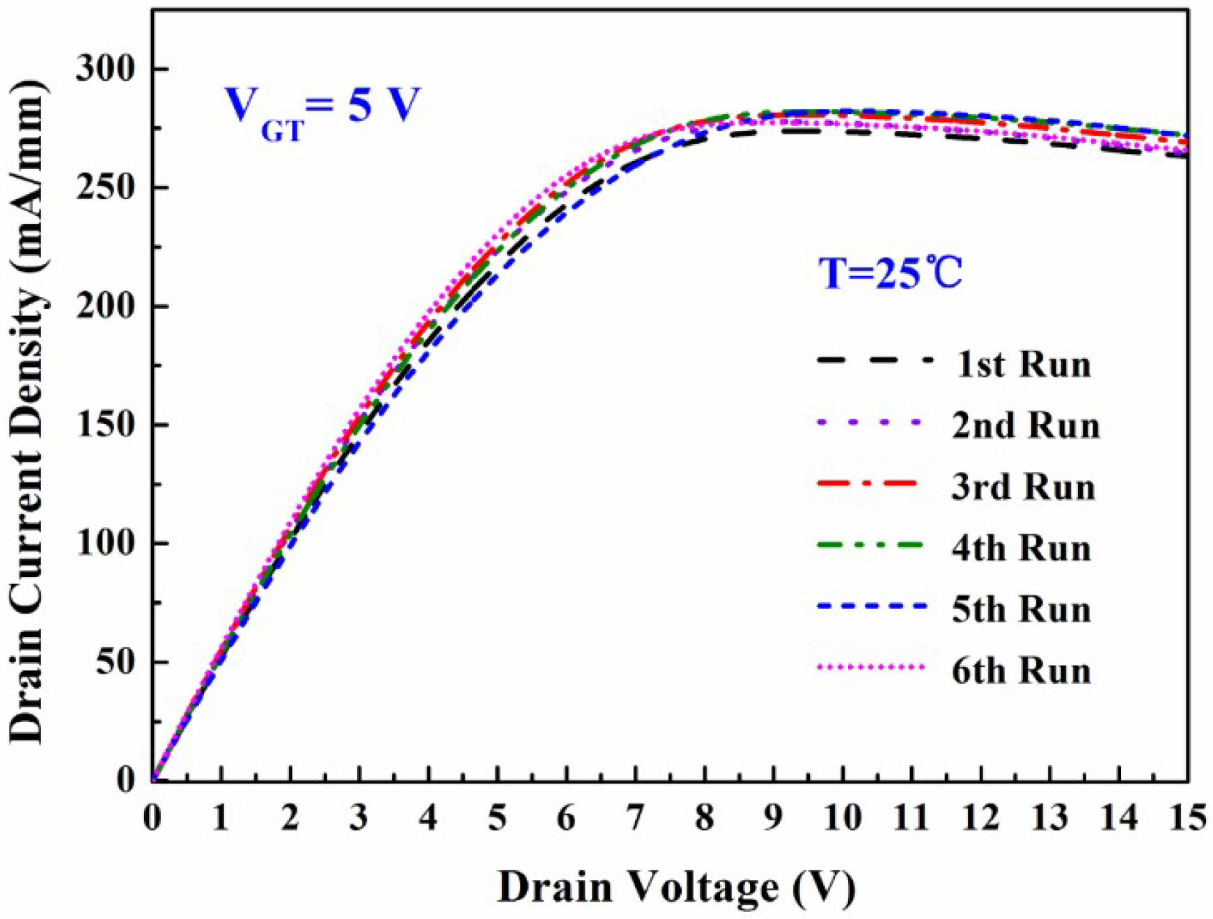
Figure 5.
Repeated measurement-dependence of the DC output characteristics in the fabricated MIS-gate HEMTs.
Figure 5.
Repeated measurement-dependence of the DC output characteristics in the fabricated MIS-gate HEMTs.

Figure 6.
Repeated measurement dependence of the typical device transfer characteristics and gate transconductance gm in the MIS-gate HEMTs at (a) 25 °C and (b) 100 °C, respectively.
Figure 6.
Repeated measurement dependence of the typical device transfer characteristics and gate transconductance gm in the MIS-gate HEMTs at (a) 25 °C and (b) 100 °C, respectively.

Figure 7.
The Vth data changed with the repeated measurement rounds in the MIS-gate HEMTs. The data were measured at gradually increasing temperatures from 25 °C to 150 °C and the measurement process was repeated for several rounds. The dotted lines and arrows show the measurement sequence.
Figure 7.
The Vth data changed with the repeated measurement rounds in the MIS-gate HEMTs. The data were measured at gradually increasing temperatures from 25 °C to 150 °C and the measurement process was repeated for several rounds. The dotted lines and arrows show the measurement sequence.

Figure 8.
Trap density data at the Al2O3/AlGaN interface employed in the analytical model and TCAD simulation, dependent on (a) the operation temperature and (b) measurement sequence.
Figure 8.
Trap density data at the Al2O3/AlGaN interface employed in the analytical model and TCAD simulation, dependent on (a) the operation temperature and (b) measurement sequence.

Figure 9.
The Vth data changed with the measurement sequence from the experimental measurement, analytical calculation using the model, and TCAD simulation work when operated at (a) 25 °C, (b) 100 °C, and (c) 150 °C, respectively.
Figure 9.
The Vth data changed with the measurement sequence from the experimental measurement, analytical calculation using the model, and TCAD simulation work when operated at (a) 25 °C, (b) 100 °C, and (c) 150 °C, respectively.


Table 1.
Summary of the typical parameters adopted in this work. 2DEG–two dimensional electron gas.
| Parameters | Descriptions | Values |
|---|---|---|
| ns | 2DEG sheet density | 6.7 × 1012 cm−2 |
| Sheet density of polarization charges at the AlGaN/GaN interface | 1.0 × 1013 cm−2 | |
| NIT | Donor-like trap density at the gate dielectric/AlGaN interface | 6.5 × 1012 cm−2 |
| µn | Electron mobility | 1050 cm2∙V∙s−1 |
| φNi | Ni work function | 5.1 eV |
| Al2O3 dielectric constant | 9.0 | |
| AlGaN dielectric constant | 10.3 (when x = 0.25) | |
| Barrier height | 1.5 eV for Schottky and 3.7 eV for MIS gates | |
| Fermi level from GaN conduction band edge | 0.39 eV | |
| Conduction band offset at the Al2O3/AlGaN interface | 1.10 eV | |
| Conduction band offset at the AlGaN/GaN interface | 0.36 eV | |
| kt | Stability coefficient | 0.75 at 25 °C; 0.32 at 100 °C; 0.15 at 150 °C |
| τn | Time constant at 25 °C | 8.6 × 10⁻⁷ s |
| NC | Conduction band state density | 2.2 × 1018 cm−3 for GaN and 4.1 × 1018 cm−3 for AlN |
| σn | Capture cross section of the traps | 1.0 × 10⁻¹³ cm2 for both GaN and AlN |
| α | Temperature coefficient | 9.09 × 10⁻⁴ eV∙K−1 for GaN and 1.80 × 10⁻³ eV∙K−1 for AlN |
© 2018 by the authors. Licensee MDPI, Basel, Switzerland. This article is an open access article distributed under the terms and conditions of the Creative Commons Attribution (CC BY) license (http://creativecommons.org/licenses/by/4.0/).
Share and Cite
MDPI and ACS Style
Huang, H.; Li, F.; Sun, Z.; Cao, Y. Model Development for Threshold Voltage Stability Dependent on High Temperature Operations in Wide-Bandgap GaN-Based HEMT Power Devices. Micromachines 2018, 9, 658. https://doi.org/10.3390/mi9120658
AMA Style
Huang H, Li F, Sun Z, Cao Y. Model Development for Threshold Voltage Stability Dependent on High Temperature Operations in Wide-Bandgap GaN-Based HEMT Power Devices. Micromachines. 2018; 9(12):658. https://doi.org/10.3390/mi9120658
Chicago/Turabian StyleHuang, Huolin, Feiyu Li, Zhonghao Sun, and Yaqing Cao. 2018. "Model Development for Threshold Voltage Stability Dependent on High Temperature Operations in Wide-Bandgap GaN-Based HEMT Power Devices" Micromachines 9, no. 12: 658. https://doi.org/10.3390/mi9120658
Note that from the first issue of 2016, this journal uses article numbers instead of page numbers. See further details here.