Abstract
Perovskite/silicon tandem solar cells are of great interest due to their potential for breaking the Shockley-Queisser limit of single-junction silicon solar cells. Perovskite solar cells are widely used as the top subcells in perovskite/silicon tandem solar cells due to their high efficiency and lower fabrication cost. Herein, we review the semi-transparent perovskite solar cell in terms of the mechanisms of their translucent structure, transparent electrodes, charge transport layer, and component modification. In addition, recent progress in the research and development of 4T perovskite/silicon tandem solar cells is summarized, with emphasis on the influence of perovskite structure and silicon cells on the progress of tandem solar cells. Finally, we discuss the challenges associated with 4T perovskite/silicon tandem solar cells and suggest directions for the development of perovskite/silicon commercialization.
1. Introduction
The demand for renewable energy has steadily increased with the transition to a carbon-neutral economy. Among various solutions, low-cost and high-performance solar cells have been considered as one of the most effective options [1,2,3,4,5]. In recent years, perovskite solar cells have emerged as a promising candidate in the photoelectric field due to their high efficiency, solution process, and low cost. Perovskite materials are widely used in various fields and have exceptional optoelectronic properties such as a high absorption coefficient [6], high carrier mobility [7], long charge diffusion length [8], and relatively expansive and tunable band gap [9].
Silicon is an important semiconductor material, and it can absorb photons with energies higher than its band gap. However, any excess energy from these photons above the band gap not only undergoes thermalization as excited electrons relax to the bottom of the conduction band, but also causes undesirable heating effects in the system. In addition, photons with energies below the bandgap are also absorbed, leading to unwanted heat generation. It is necessary to balance the capture of photons with the minimization of thermalization losses. After more than 70 years of development, the laboratory efficiency of silicon solar cells has reached 27%, which is close to the theoretical Shockley-Queisser (SQ) efficiency limit of 29.4% [10,11]. More importantly, perovskite solar cells (PSCs) have achieved a record efficiency of 26.1%, which is comparable with Si solar cells [12].
Several innovative physical concepts such as multi-junction solar cells, hot carrier solar cells, multiple exciton generation, and intermediate band solar cells have been proposed to overcome the Shockley-Queisser limit in solar cells. Among these concepts, multi-junction cells have been experimentally proven to overcome the development bottleneck. A GaAs/GaInP/Ge triple-junction solar cell has been shown to achieve an efficiency above 40% under concentrated sunlight by using three component cells with different band gaps. Multijunction cells optimize photon absorption by utilizing different bandgaps, resulting in higher Voc and broader spectrum utilization [13]. Among them, perovskite/silicon tandem solar cells have greatly promoted the development of highly efficient multi-junction solar cells. The combination of PSCs and silicon cells enable more efficient utilization and break the SQ efficiency limit of single-junction cells, further promoting the industrialization of perovskite solar cells. The efficiency chart of reported ST-PVK solar cells and 4T PVK/Si tandem solar cells is shown in Figure 1.
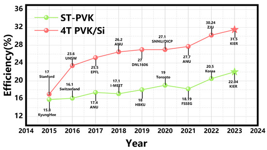
Figure 1.
The efficiency chart of reported ST-PVK solar cells and 4T PVK/Si tandem solar cells.
Typical perovskite/silicon (PVK/Si) tandem solar cells include two structures: a four-terminal (4T) mechanically integrated structure and a two-terminal (2T) monolithically integrated structure, as shown in Figure 2 [14,15]. For 2T PVK/Si tandem solar cells, the current alignment is governed by Kirchhoff’s law. This law states that the photocurrent is limited by the subcell with the lower current. To achieve matched photocurrents at the maximum power point, it is essential to design the bandgap and thickness of each subcell. However, the manufacturing process of 2T multijunction cells is much more complex than that of 4T tandem solar cells. The surface conditions of the bottom cell directly affect the film quality of the top cell. It is a significant challenge to prepare high quality perovskites on the textured Si cell in 2T tandem solar cells [16].
To overcome these challenges, 4T perovskite/silicon tandem solar cells have been developed, using a mechanically stacked top and bottom cell. One of the attractive advantages of this cell type is that current alignment is not necessary for 4T perovskite/silicon tandem solar cells. In addition, it is easy to modify the transmittance of perovskites by altering the film thickness. Moreover, the 4T PVK/Si tandem solar cells exhibit an independent process for subcells, and the subcells are optically coupled without any electrical connection [16,17]. Importantly, degraded perovskite subcells in 4T PVK/Si tandem solar cells can be replaced efficiently, which improves the potential of 4T PVK/Si tandem solar cells. The theoretical efficiency of 4T PVK/Si tandem solar cells is expected to reach 45% (Figure 2e) [18,19,20].
This work reviews recent progress in the development of ST-PVK and 4T PVK/Si tandem solar cells. The mechanisms of the translucent structure, transparent electrodes, charge transport layer, and component modification in ST-PVK solar cells is systematically summarized. The development and challenges of 4T PVK/Si tandem solar cells are further discussed.
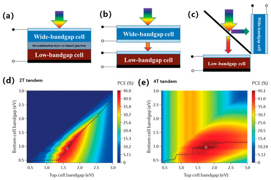

Figure 2.
Schematic structure of a tandem solar cell: (a) 2T monolithically integrated. (b) 4T mechanically integrated. (c) 4T optical spectral splitting. (d,e) Theoretical maximum PCE for 2T and 4T PVK/Si tandem solar cells [21]. Reproduced with permission: Copyright 2019, John Wiley and Sons.
Figure 2.
Schematic structure of a tandem solar cell: (a) 2T monolithically integrated. (b) 4T mechanically integrated. (c) 4T optical spectral splitting. (d,e) Theoretical maximum PCE for 2T and 4T PVK/Si tandem solar cells [21]. Reproduced with permission: Copyright 2019, John Wiley and Sons.
2. Translucent Structure Mechanisms
ST-PSCs are widely used to enhance light operational capability and fabricate tandem solar cells. The structure of a ST-PSC directly affects its efficiency, transparency, and stability. Therefore, it is essential to design a novel translucent structure and modify the thickness of the perovskite film. The band gap of perovskites is modified using the component ratio of halide elements (bromide, iodide, and chloride) [22]. It has been found that the transparency of MAPb(I3−xBrx)3 perovskite can be adjusted by altering the ratio of bromide and iodide, where x ranges from 0 to 3. Using more bromide for a constant film thickness can achieve a higher average transparency. For a 300 nm film, the average transparency ranges from 10% AVT to 24% [23]. Figure 3a shows that the absorption spectra shifts to a short wavelength with additional bromide due to a wider band gap, resulting in decreased PCE due to spectral losses. However, optimizing bromide content could enhance perovskite film crystallinity and photovoltaic performance. Another strategy for achieving semi-transparency is to adjust the thickness of the film by changing the concentration of the solution with a constant bromide ratio. Thinner films may allow partial light transmission depending on absorption coefficient and wavelength [24]. A common approach to fabricating semi-transparent perovskite cells involves thinning the film via low perovskite solution concentration. However, the lower solution concentration process usually exhibits sub-optimal film coverage and pinhole problems. Quiroz et al. proposed two fine-tuning approaches that maintain crystallinity and film quality to address these issues [25]. The first approach is solvent-induced rapid crystallization deposition combined with nitrogen flow quenching. The second approach is the solvent extraction method, which produces active layers as thin as 40 nm by fast crystal deposition, as shown in Figure 3b. Improved deposition techniques, such as vacuum deposition, allow for precise control of the perovskite film thickness by adjusting the deposition rate. Roldan-Carmona et al. [26] achieved a higher AVT of 22% and a PCE of 7.3% using co-evaporation of CH3NH3I and PbI2 with an active layer thickness of 100 nm, as shown in Figure 3c. Chen et al. developed a dual-source vacuum co-evaporation process to fabricate CsPbBr3 thin films for planar architecture devices [27]. The dual-source vacuum co-evaporation process involves simultaneous evaporation of CsBr and PbBr2, followed by annealing to achieve a single-phase perovskite structure. The evaporation rate is a critical parameter to modify the crystallinity, grain size, and film thickness. The perovskite films produced by dual-source vacuum co-evaporation are of high quality with no pinholes. The corresponding semi-transparent CsPbBr3 solar cells have been shown to achieve a PCE of 5.98%. Surface treatment and additives engineering help to improve the ultra-thin coverage and uniformity of perovskite films. Bag et al. [28] obtained chalcogenide compounds from thiourea vapor and fabricated uniformly prepared perovskite film with a thickness of 110 nm, as shown in Figure 3d. Guo et al. introduced polyvinylpyrrolidone (PVP) as an additive in preparing perovskite precursors and achieved a PCE of 5.36% with an active layer thickness of 90 nm, shown in Figure 3e [29]. Recently, Wen et al. introduced dicyandiamide (DCD) as an antioxidant additive to further improve film quality [30]. The robust coordination bond between DCD and Pb/Sn could prevent Sn2+ oxidation at low temperatures. The optimized ST-PSCs achieved a higher PCE of 14.17% with an active area of 0.1 cm2, as shown in Figure 3f. Pon et al. prepared low-dimensional perovskite films with the composition (PEA)2(MA)n−1PbnIn+1Br2n, where n = 1, 3, and 5. They found that the transparency of the films decreased as the value of n increased, as shown in Figure 3g [30]. Reducing the thickness of the photoactive layer increases the permeability; however, a thinner layer absorbs less light, resulting in a lower device short-circuit current. Zhang et al. fabricated compact and ultrathin perovskite films through thermal evaporation (Figure 3h) [31]. The films had a smooth surface and directional crystal growth, resulting in 10 nm thin films with a compact and continuous morphology and without any pinholes. Furthermore, low-dimensional perovskites (R2n−1BnX3n+1) are widely used as the absorbing layer in ST-PSCs. Yao et al. demonstrated that the introduction of ADDC could convert harmful I2 to I− in the precursor solution, reducing the deep-level trap density in perovskite films. They achieved a high-performance semi-transparent PSC with an impressive PCE of 18.6% and a remarkable Voc of 1.24 V [32].
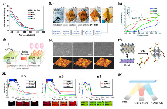
Figure 3.
Schematic diagram of achieving semitransparency by modulating perovskite thickness. (a) Absorbance spectra of MAPb(I3−xBrx)3 perovskite films with varying bromine content (x) [23]. (b) Schematic representation of the SEE method showing a 5-s crystallization process [25]. Reproduced with permission: Copyright 2012, Royal Society of Chemistry. (c) Transmittance spectra of different thicknesses of perovskite layers on transparent electrodes, indicated by solid and open circles [26]. Reproduced with permission: Copyright 2008, Royal Society of Chemistry. (d) Schematic diagram of the PEDOT:PSS surface passivation by thiourea [28]. Reproduced with permission: Copyright 2016, Elsevier Ltd. (e) Surface morphology SEM is shown at the top, and AFM is at the bottom [29]. Reproduced with permission: Copyright 2016, John Wiley and Sons. (f) Schematic diagram of DCD molecular structure [30]. Reproduced with permission: Copyright 2023, Elsevier Ltd. (g) The UV-Vis absorption spectra and film images of (PEA)2(MA)n−1PbnIn+1Br2n perovskite thin films (n = 1, 3, and 5) [31]. Reproduced with permission: Copyright 2011, Royal Society of Chemistry. (h) Schematic illustration of perovskite film deposition via thermal evaporation method [33]. Reproduced with permission: Copyright 2023, John Wiley and Sons.
Wide band gap perovskite films usually exhibit a yellowish-brown or reddish-brown hue. However, neutral colors can be achieved by creating microstructures in the fully transparent area of the perovskite material. The perovskite microstructure can be obtained through a dehumidification strategy and microscopic mold. Giles et al. [34] created islands of perovskite microstructure by using an excess of organic matter and a solvent with a low vapor pressure. The solvent slowed perovskite crystallization, resulting in discontinuous islands. Furthermore, they illustrated the simple coloring of these cells through dye incorporation without any reduction in performance. The efficiency of the champion device was 3.5%, as depicted in Figure 4a,b. Chen et al. utilized Pb(SCN)2 as a lead source with excess CH3NH3I to create microstructural islands in semi-transparent CH3NH3PbI3 solar cells [35]. The high Pb(SCN)2 content was shown to improve film transmittance, and obtained a PCE of 11.6%, as presented in Figure 4c. However, semi-transparent devices with island microstructures exhibited a lower Voc due to the incomplete separation of the electron and hole transport layers. Hörantner et al. employed a lithographic method to optimize perovskite crystallization, preventing direct contact between the transport layers and perovskite film. This improvement of film crystallization increased the performance of perovskite solar cells [36].
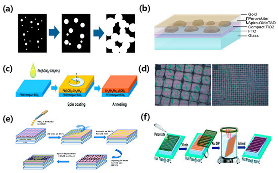
Figure 4.
(a) Schematic diagram depicting the temporal evolution of the film wetting process. The perovskite material is depicted in black, while the white areas denote the presence of pores. (b) Schematic diagram illustrating the structural arrangement of a wet planar perovskite heterojunction solar cell [34]. Reproduced with permission: Copyright 2014, American Chemical Society. (c) Illustration of the formation of microstructural islands in CH3NH3PbI3 semitransparent solar cells using Pb(SCN)2 as the lead source in conjunction with excess CH3NH3I [35]. Reproduced with permission: Copyright 2016, Royal Society of Chemistry. (d) Optical microscope image of the wide grid and optical microscope image of the dense grid [37]. Reproduced with permission: Copyright 2015, John Wiley and Sons. (e) Schematic of the ST-PVK solar cell made by a two-step deposition process [38]. Reproduced with permission: Copyright 2016, Royal Society of Chemistry. (f) Illustration demonstrating the formation of a perovskite grid using the 1.5-step deposition method [39]. Reproduced with permission: Copyright 2013, Royal Society of Chemistry.
Perovskite materials have been widely used in absorbing layers due to their self-assembly process with wet deposition methods [26,40]. Aharon et al. fabricated a semi-transparent perovskite solar cell based on mesoporous TiO2 and achieved a PCE of 0.4–5%, as shown in Figure 4d [37]. Rahmany et al. further developed the self-assembly process of perovskite lattices using a two-step deposition method and induced mesoporous TiO2 and Al2O3 NPs as electron transport layers (ETL). The device with the optimum PbI2 concentration of 0.5 M achieved a PCE of 8% due to the increased film coverage. A transparent DMD back contact was utilized to fabricate semi-transparent device and achieve a PCE of 5.5%, as shown in Figure 4e [38]. Rai et al. improved the perovskite film quality by using a mixed cation, Cs0.2FA0.8Pb(I0.6Br0.4)3. The dipping of the hot FAI solution could promote the formation of the grid and improve device performance and stability, as illustrated in Figure 4f [39].
3. Transparent Electrodes
The ideal transparent electrode for ST-PVK solar cells should possess high optical transmittance in the visible and near-infrared spectrums, low resistivity, and compatibility with adjacent layers. Due to the ordinary thermal stability of perovskites, it is preferable to use low-temperature processes for electrode deposition [41,42,43]. Various electrode technologies have been developed to further improve the efficiency of perovskite solar cells, including silver nanowires, carbon nanomaterials, ultrathin metals, conductive polymers, and transparent conductive oxides. This article provides an overview of transparent electrode applications and optimization scenarios in ST-PSCs.
3.1. Silver Nanowires
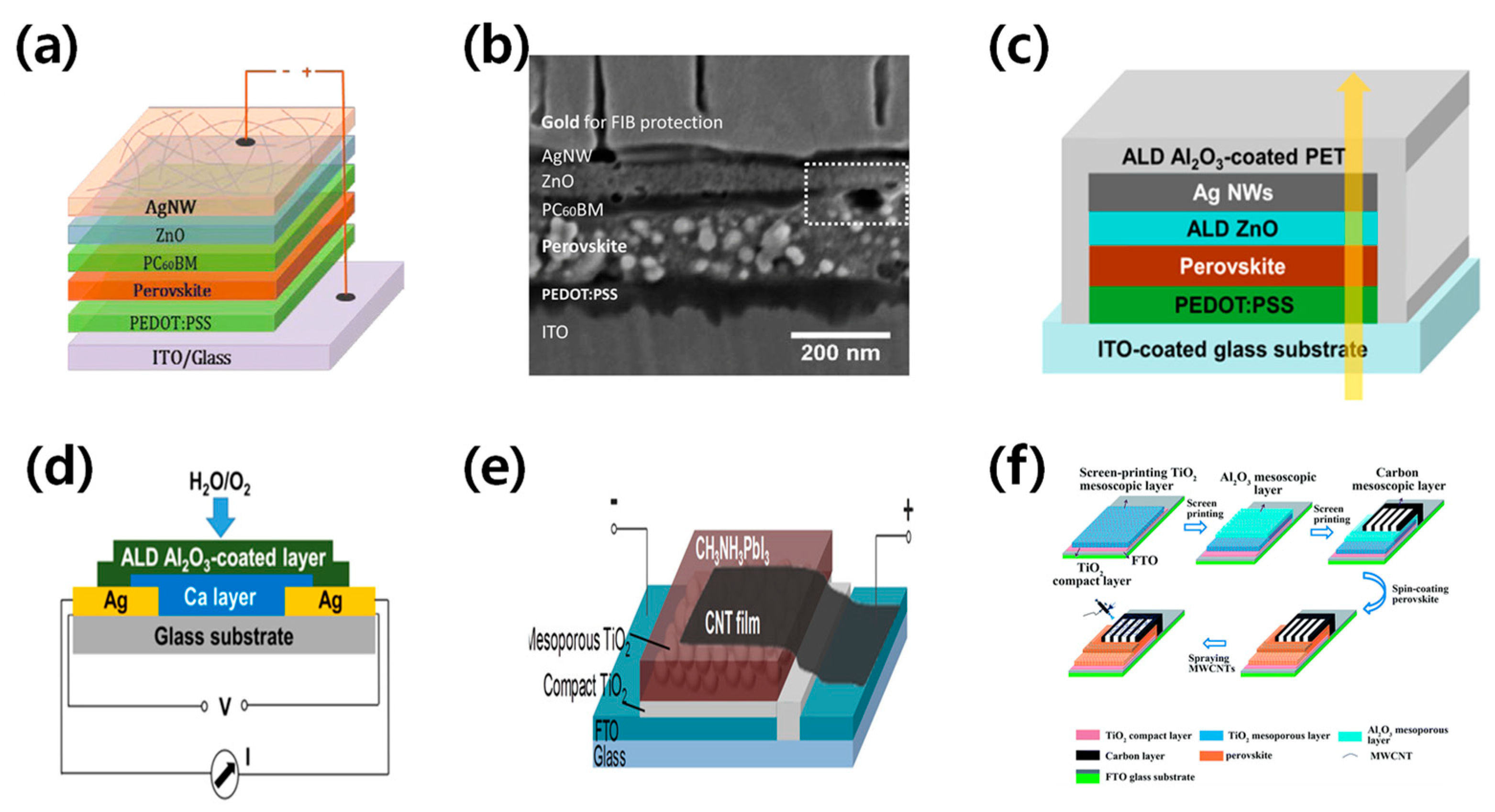
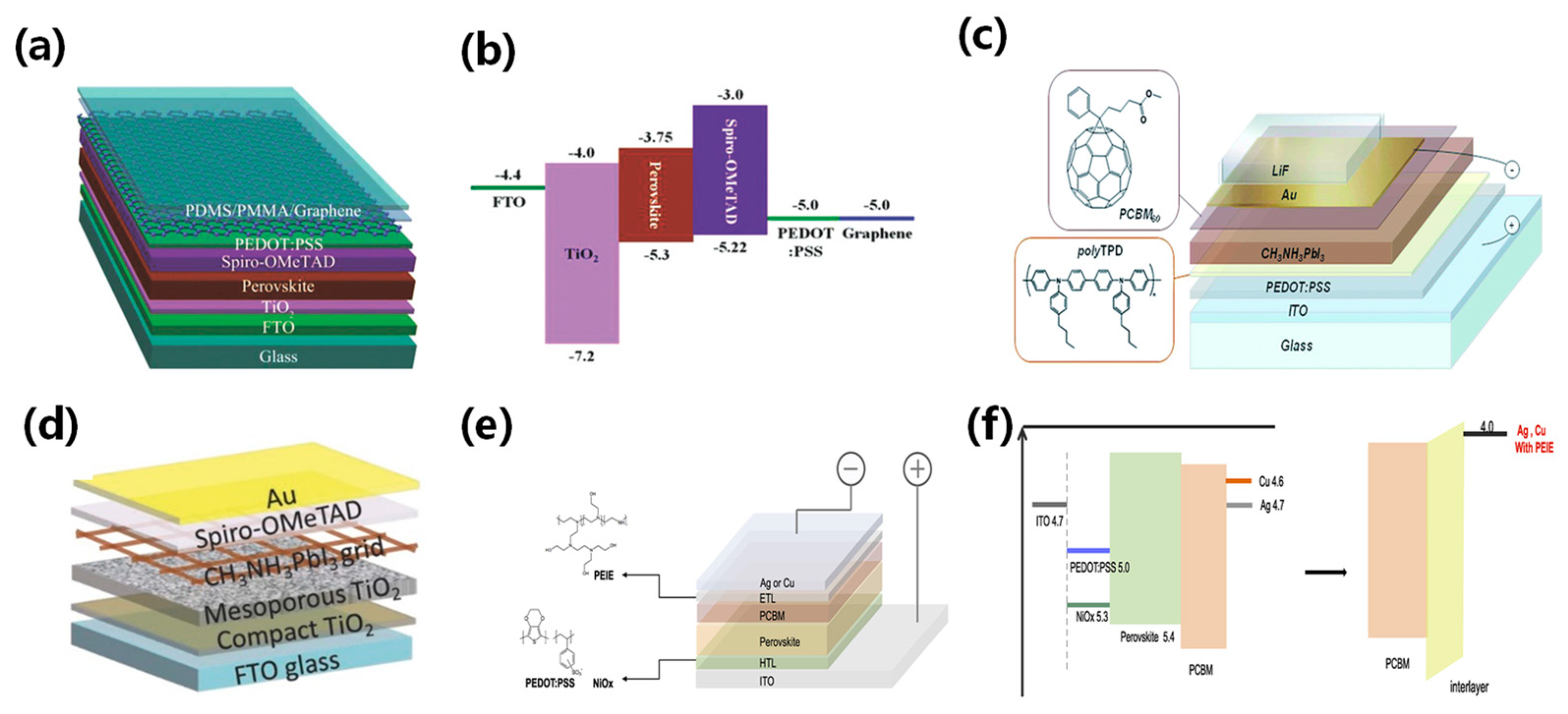
Silver nanowires (AgNWs) are becoming increasingly popular as a substitute for ITO electrodes due to their superior mechanical and optoelectronic properties, and ability to be produced on a large scale. The performance of AgNWs is influenced by their diameter, length, area density, and interconnection, which affect their transmittance, resistance, and haze [44]. Guo et al. successfully produced efficient perovskite solar cells using AgNWs processed in a solution process as electrodes [45]. Spraying isopropanol-diluted AgNWs showed low resistance and high transmittance and the champion device with a ZnO layer achieved a PCE of 8.5%, as shown in Figure 5a,b. Chang et al. fabricated semi-transparent perovskite solar cells with an efficiency of 10.8% using solution-processed AgNWs [46]. They fabricated ZnO thin films using ALD as a buffer, along with electron transport layers to further increase the charge transport. To prevent oxidation and corrosion of AgNWs, the ALD-deposited Al2O3 thin film was induced as a protective layer. This strategy could significantly improve device stability while affecting efficiency and transparency, as shown in Figure 5c,d. Hong Lin’s team proposed an Au/AgNWs bilayer electrode to prevent halide migration from the perovskite by separating the AgNWs from the halides. The authors used a 6 nm Au layer–AgNWs combination to improve the orientation of the spin-coated AgNWs layers and achieve a high fill factor. Their semi-transparent perovskite solar cell achieved an impressive PCE of 11%.

Figure 5.
(a) Schematic structure of the devices with solution-processed top AgNWs. (b) Cross-sectional image of the whole device stack. The white dashed rectangle shows the area where PC60BM does not cover perovskite [45]. Reproduced with permission: Copyright 2009, Royal Society of Chemistry (Great Britain) and Guo jia na mi ke xue zhong xin (China). (c,d) Schematic illustration of the semitransparent device architecture, with ZnO thin film deposited by atomic layer deposition (ALD) as the buffer and electron transport layer. The yellow arrow refers to sunlight direction [46]. Reproduced with permission: Copyright 2015, American Chemical Society. (e) Schematic illustration of a CH3NH3PbI3 perovskite solar cell with carbon nanotube (CNT) film electrode [47]. Reproduced with permission: Copyright 2014, American Chemical Society. (f) Schematic illustration of coating thin-layer multi-wall carbon nanotubes (MWCNTs) to produce an ST-PVK solar cell [48]. Reproduced with permission: Copyright 2013, Royal Society of Chemistry.
3.2. Carbon Nanomaterials
Carbon nanomaterials are widely used as electrodes due to their low-cost, stable, and hydrophobic transparency, which requires improved conductivity and optical transmittance. Zhen et al. synthesized CNT films by using the chemical vapor deposition method and pressed them directly onto perovskite cell layers [49]. The fabricated ST-PSCs without a hole transport layer achieved a PCE of 6.29%. However, the optical transmittance of these films was lower than FTO, as shown in Figure 5e [47]. Li et al. [48] fabricated ST-PVK solar cells with using a carbon lattice as the top transparent electrode. The corresponding ST-PSCs obtained a PCE of 11.31% at minimal grid spacing. In addition, the thin layer of multi-wall carbon nanotubes (MWCNTs) fabricated with spray coating could achieve an efficiency of 8.21% with a transparency of 24.0%, as shown in Figure 5f.
Graphene is a popular candidate for transparent electrodes due to its high carrier mobility and superior optical properties. It has a lower absorption rate of only 2.3% over a broad solar spectrum [50]. Feng et al. fabricated graphene electrodes on copper foil using CVD and transferred them to perovskite solar cells. To further enhance the conductivity of the graphene electrodes, they deposited a layer of PEDOT:PSS. The device performance was further enhanced by altering the layers and conductivity of the graphene electrodes, as shown in Figure 6a,b [51].
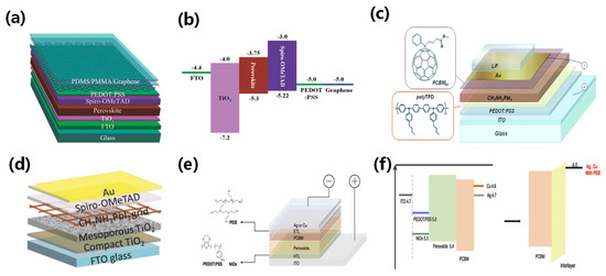
Figure 6.
(a) Schematic illustrating the fabrication of graphene transparent electrodes on copper foil using the chemical vapor deposition (CVD) method, and (b) the band structure of the device [51]. Reproduced with permission: Copyright 2015, John Wiley and Sons. (c) Schematic layout of the semi-transparent solar cell and chemical structures of the organic hole and electron-blocking materials [26]. Reproduced with permission: Copyright 2008, Royal Society of Chemistry. (d) Schematic illustration of semi-transparent perovskite devices using screen-printed stainless-steel mesh and wet deposition techniques [37]. Reproduced with permission: Copyright 2015, John Wiley and Sons. (e) Structure diagram of semi-transparent perovskite solar cell with Ag or Cu as a transparent electrode and (f) energy band diagram [52]. Reproduced with permission: Copyright 2019, Elsevier Ltd.
3.3. Ultrathin Metals
Ultrathin metal films are well-suited for large-area device manufacturing due to their excellent conductivity. In traditional PSCs, metal electrodes are opaque and require significant thickness reduction to achieve transparency. Several studies on ST-PSCs have reported thin metal films (such as Al, Ag, and Au) fabricated via an evaporation method as their top electrodes [26,34,53]. Roldán-Carmona et al. presented a semitransparent perovskite solar cell based on the inverted structure [26]. They used ultrathin gold as the top electrode and enhanced transparency by minimizing mirror-reflection-induced energy loss via a LiF layer. The team created a thin and uniform perovskite absorption layer using a thermal evaporation method, further boosting transparency under low temperatures. Figure 6c shows that devices with an average transmittance of 29% achieved an efficiency of 6.4%, whereas devices with a transmittance of 22% exhibited a PCE of 7.3%. Sigalit et al. improved the transparency of semi-transparent perovskite solar cells by using a silkscreen-printed stainless-steel net and wet deposition technology for perovskite grid creation [37]. The device transparency was controlled by altering the perovskite solution concentration and grid hole opening. This work presented a controlled patterned perovskite layer to produce semitransparent cells. Through adjusting the concentration of the perovskite solutions and the size of the grid holes, the semitransparent solar cell achieved an efficiency of 5%, as shown in Figure 6d. Lee et al. investigated the difference between Ag and Cu as semi-transparent top electrodes in semi-transparent perovskite solar cells (ST-PSCs) [52]. They found that Cu has lower thin-film resistance than Ag, while maintaining comparable transparency (Figure 6e,f). Chen et al. utilized an ultrathin silver film as the top transparent electrode in perovskite solar cells and introduced a tellurium oxide layer to boost light absorption and transmittance [54]. The TeO2/Ag electrode significantly enhanced short-circuit current and efficiency. Their device achieved high bifacial PCEs of 21%, excellent reproducibility, and stable performance.
Ultrathin metal electrodes usually do not meet conductivity and optical transmittance requirements. Thus, it is necessary to balance conductivity and optical transmittance. The metal layer is responsible for the excellent conductivity, while the transparency of the electrode is improved by interference and anti-reflection at the multi-layer interfaces. Della et al. fabricated efficient perovskite solar cells with a transparent DMD (MoO3/Au/MoO3) electrode [55]. The DMD structure, which contains interference effects between two dielectric layers, enhances electrode transmittance. The research optimized the layer thickness, resulting in a DMD electrode square drop to 13 Ω and a higher efficiency of 13.6%, as shown in Figure 7a. A thin Au layer was introduced into the DMD structure to further achieve excellent optical transparency and electrical conductivity. MoOx/Au/Ag arrangement exhibited optimized band matching and increased the hole transport rate. The semitransparent perovskite solar cell with the DMD electrode structure achieved an efficiency of 11.5%, as shown in Figure 7b [56].
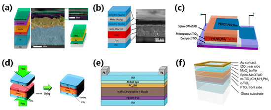
Figure 7.
(a) Structure diagram, SEM image, and DMD transparent electrode perovskite magnification [55]. Reproduced with permission: Copyright 2015, Elsevier Ltd. (b) MoOx/Au seeded Ag layer/MoOx structure diagram and TEM image of the transparent electrode [56]. Reproduced with permission: Copyright 2015, American Chemical Society. (c) Transfer lamination using PEDOT:PSS films for perovskite structure diagram [57]. Reproduced with permission: Copyright 2015, American Chemical Society. (d) Schematic illustration of device fabrication and architecture of a MAPbI3 planar sandwich solar cell [58]. Reproduced with permission: Copyright 2008, Royal Society of Chemistry. (e) Device structure diagram of ITO/ZnO nanoparticle electrode prepared using ZnO nanoparticle as a buffer layer [59]. Reproduced with permission: Copyright 2016, John Wiley and Sons. (f) Schematic illustration of a perovskite solar cell structure with a transparent rear electrode and Au contact [60]. Reproduced with permission: Copyright 2015, Elsevier B.V.
3.4. Conductive Polymers
PEDOT:PSS is commonly used as a transparent electrode in ST-PSCs due to its high transmittance and conductivity. However, the hygroscopicity of PEDOT:PSS could potentially damage perovskite film, which has limited its application in perovskite solar cells [61,62]. In 2015, Bu et al. applied PEDOT:PSS thin films on perovskite solar cells using transfer lamination and achieved an increased efficiency of 11.29% [57]. Furthermore, similar techniques resulted in a semi-transparent perovskite cell that achieved an efficiency of 10.1%, with a transmittance of 7.3% between 370–740 nm, as illustrated in Figure 7c. They utilized a transfer lamination technique with plastic packaging as the transfer medium to produce large-area PEDOT:PSS transparent electrodes.
3.5. Transparent Conductive Oxides (TCO)
Transparent conductive oxides (TCOs) showed significant electronic and optical characteristics, including transmittance of over 85%, marking them as prominent transparent electrodes. The most commonly used TCOs are indium tin oxide (ITO), indium zinc oxide (IZO), and aluminum-doped zinc oxide (AZO). TCOs are usually deposited through sputtering methods, but this method can potentially harm the perovskite absorptive layer [63,64]. Refining the deposition techniques can protect the underlying materials when employing regulated sputtering parameters to mitigate damage to the electrode layer. Heo et al. laminated PEDOT:PSS as the interface layer on ITO transparent electrodes to fabricate semitransparent perovskite solar cells. The device using P3HT for hole transport achieved efficiencies of 12.8% due to its strong light absorption. Conversely, those using PTAA registered a higher efficiency of 15.8%, as shown in Figure 7d [58]. A suitable buffer between the perovskite absorbing layer and the TCO electrode can reduce sputtering damage. Bush et al. fabricated ITO/ZnO dual layers with ZnO nanoparticles as the buffer layer. However, significant interface potential barriers existed at the interface due to the unmatched work functions of ZnO and ITO, hindering electron extraction. Using AZO nanoparticles that match the ITO work function as the buffer layer, the researchers overcame the barriers and improved device efficiency [59]. With an inverted structure, the resulting semitransparent perovskite solar cell achieved an efficiency of 12.3%, as shown in Figure 7e [59].
IOH/ITO is another TCO that has received significant attention. Werner et al. used thermal evaporation to create a 10 nm molybdenum oxide protective layer and introduced a 110 nm thick IOH/ITO transparent conductive film primer via sputtering. They achieved an efficiency of 14.5% for the single-junction semi-transparent perovskite solar cell by tuning all layer thicknesses and using the perovskite absorption layer fabrication method [65]. IZO and AZO films showed high transmittance in the long-wave range, making them suitable for transparent electrodes with high mobility. Werner et al. fabricated a 120 nm IZO transparent electrode using sputtering, achieving a high transmittance of 97% in the 400–1200 nm range. After integrating a molybdenum oxide buffer, the semi-transparent perovskite solar cell with IZO improved efficiency from 9.7% to 10.3%, as shown in Figure 7f [60]. Wahl et al. fabricated an inverted semitransparent perovskite solar cell by sputtering IZO directly onto the electron transport layer, and achieved an efficiency of 13% [66]. Fu et al. fabricated a 400 nm AZO transparent electrode via sputtering and obtained an higher efficiency of 16.1% with an average transmittance of 80.4% within the 800–1200 nm range [67]. Yoon et al. fabricated a semitransparent perovskite solar cell using gallium- and titanium-doped indium oxide (IO:GT) between the electron transport layer and the transparent electrode and increased the power conversion efficiency of ST-PSC from 8.59% to 17.90% [68]. The device performance of ST-PVK solar cells is summarized in Table 1.

Table 1.
Summary of semi-transparent perovskite solar cells.
Ideally, transparent electrodes should have several key properties for semi-transparent perovskite and tandem solar cells. Transparent electrodes are expected to fabricate at low temperatures, and exhibit excellent electrical conductivity, high optical transparency, good chemical stability, and compatibility with adjacent layers. Silver nanowires (AgNWs) have gained attention due to their desirable properties, including high electrical conductivity and optical transparency of up to 90%. They can be easily synthesized with a large-scale solution-based method. However, a major drawback is the reaction between AgNWs and halide ions in perovskite materials, leading to the formation of silver compounds. The reaction will form harmful AgI, leading to a degradation in device performance. Carbon nanotubes (CNTs) are a good candidate for transparent electrodes due to their excellent electrical conductivity and stability. However, the transparency of CNTs is lower than other materials, and they exhibit higher resistance. Graphene has good optical transparency, but poor stability and electrical conductivity. When considering ultra-thin metal electrodes, it is necessary to incorporate suitable buffer layers to achieve a balance between these properties. Furthermore, the implementation of a DMD structure has shown promise in improving the stability of ultra-thin metal electrodes. Conductive polymers represent another option for transparent electrode materials. They can be synthesized using cost-effective solution-based methods, but their environmental stability is limited. Transparent conducting oxides (TCO) are the most common transparent electrodes due to their high electrical conductivity and optical transparency. To prevent damage to the perovskite absorber layers, it is necessary to incorporate suitable buffer layers between the perovskite absorber and TCO electrode interfaces when directly sputtering TCO onto them.
4. Charge Transport Layer Regulation
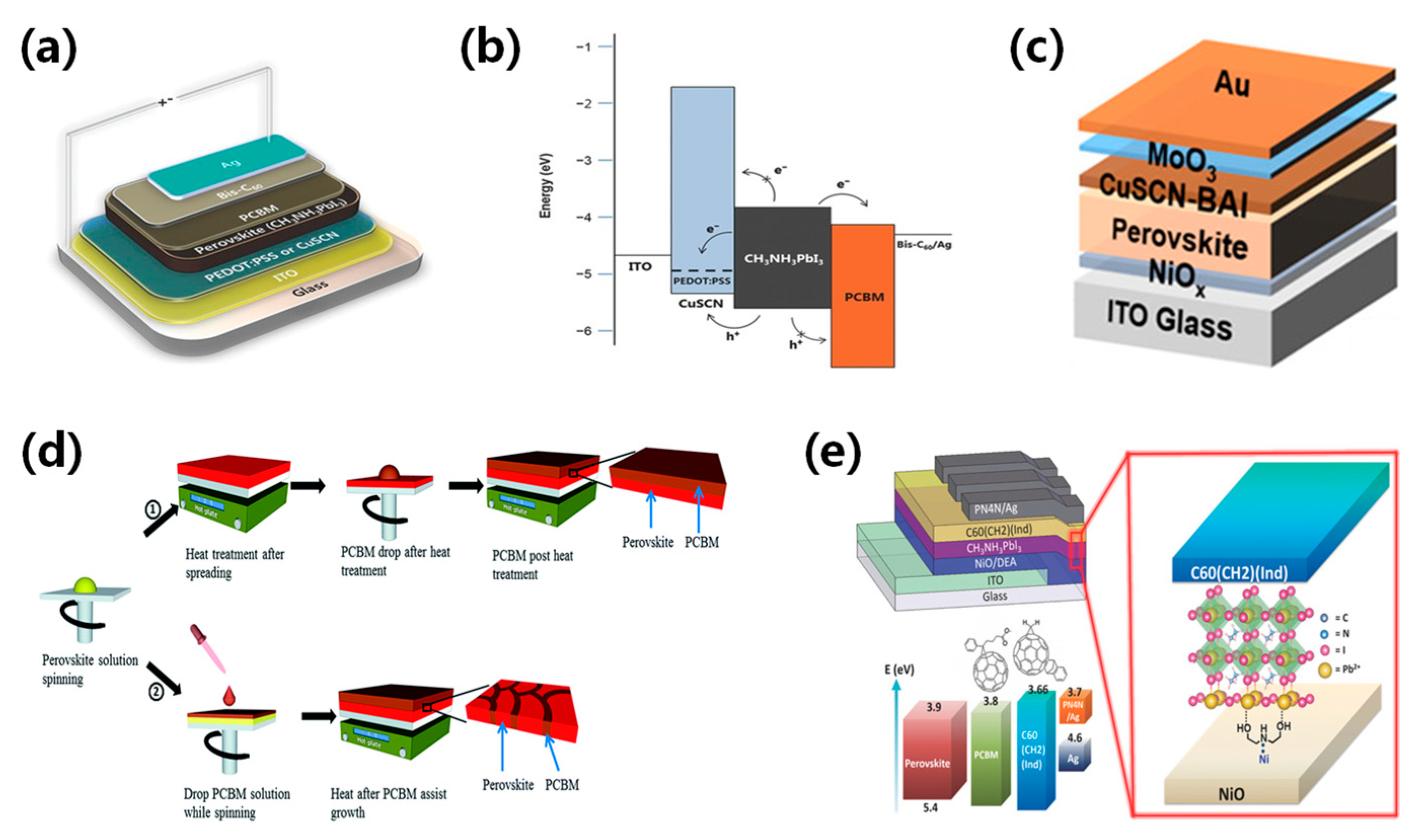
The efficiency of perovskite solar cells is related to the mobility and work function of the charge transport layer. The appropriate selection of charge transport layer could significantly enhance carrier transport and device performance. It is important to incorporate a charge transport layer with good conductivity and strong energy level alignment with the perovskite. Jae et al. substituted the typical PEDOT:PSS with CuSCN as the hole transport layer and employed CH3NH3PbI3 as the perovskite absorber layer, resulting in ST-PSCs with a PCE of 10% [89]. The valence band of CuSCN is well aligned with that of CH3NH3PbI3, minimizing the barrier for effective charge extraction, as shown in Figure 8a,b. Sun et al. described an additive engineering strategy to enhance the p-type conductivity of CuSCN HTLs [72]. The introduction of n-butylammonium iodide could increase Cu2+ formation and the number of Cu vacancies, boosting hole concentration and conductivity. Additionally, this additive promoted the solubility of the CuSCN precursor solution, resulting in a uniform layer and a high PCE of 19.24%, as shown in Figure 8c. Recently, Jeong et al. proposed a device architecture for sputtering damage-free semitransparent perovskite solar cells (PSCs) [73]. In this architecture, a p-type NiOx nanoparticle overlayer on perovskite acts as a hole transporting and buffer layer to avoid sputtering damage. The NiOx-based semi-transparent PSCs exhibited exceptional durability, achieving a PCE of 19.5%.

Figure 8.
(a) Device structure diagram and (b) band diagram of solution-treated CuSCN as the hole transport layer [89]. Reproduced with permission: Copyright 2015, John Wiley and Sons. (c) The device structure diagram of BAI as a CuSCN hole transport layer additive [72]. Reproduced with permission: Copyright 2022, American Chemical Society. (d) Diagram depicting the process flow for device fabrication: ① Conventional growth leading to distinct perovskite and PCBM layers, and ② PCBM-assisted growth resulting in a perovskite-PCBM hybrid structure [90]. Reproduced with permission: Copyright 2013, Royal Society of Chemistry. (e) Device configuration of inverted planar perovskite solar cells, along with C60(CH2) (Ind) as the electron transport layer (ETL) and the surface modifier (DEA) for NiO anode modification [91]. Reproduced with permission: Copyright 2016, John Wiley and Sons.
Currently, titanium dioxide (TiO2), tin dioxide (SnO2), and zinc oxide (ZnO) are widely used as electron transport layers. In inverted perovskite solar cells, the electron transport layer usually adopts n-type organic semiconductors like fullerene and its derivatives, which possess excellent film uniformity and electron mobility. Li et al. developed semi-transparent perovskite solar cells by using a simple low-temperature PCBM-assisted perovskite growth method [90]. The devices exhibited good transparency in the visible light wavelength range and achieved a PCE of 9.1%, as shown in Figure 8d. Xue et al. [91] used fullerene derivative as an electron transport layer and NiOx as a hole transport layer to achieve a PCE of 12.6%, as shown in Figure 8e. Recently, Yu et al. adopted ALD SnOx as a buffer layer to avoid sputtering damage and achieved a PCE of 20.25% [84]. Meanwhile, they found that the conventional PCBM inhibits ALD SnOx layer-by-layer growth, whereas introduced reaction sites activate the PCBM layer.
5. Component Modification
The four-terminal perovskite/silicon tandem solar cells provide a significant advantage given their independent subcells. The band gap of perovskites for 4T perovskite/Si tandem solar cells exhibit a large range from 1.5 eV to 1.79 eV. Along with the band gap, optical coupling is important to increase the performance of tandem solar cells. Furthermore, perovskite materials are crucial in enhancing solar cell efficiency. Table 1 summarizes the components of semi-transparent perovskite solar cells with different band gaps. MAPbI3 is firstly used alongside semi-transparent perovskites with a band gap of 1.55 eV due to its sample film process and excellent performance. Bailie et al. fabricated a 4T perovskite/silicon tandem solar cell with a PCE of 17% based on MAPbI3 perovskites [41]. Ren et al. fabricated a perovskite top cell with MAPbI3 components and combined it with PERC solar cells to achieve a tandem solar cell with a PCE of 22.4% [92]. Wide band gaps could obtain high efficiency with a large Voc and thin perovskite film, which could promote silicon to absorb more light and achieve high tandem efficiency. Additionally, the addition of Cs and FA could significantly enhance the stability of wide-bandgap solar cells. Yoon et al. fabricated FA0.87Cs0.13Pb(I0.87Br0.13)3 perovskite as top subcell and combined it with gallium and titanium-doped indium oxide (IO:GT) as a transparent electrode to achieve a tandem PCE of 23.35% for a four-terminal tandem solar cell [68]. The all-inorganic perovskite cell CsPbBr3 with a bandgap of 2.3 eV can also serve as the top cell in 4T perovskite/Si tandem solar cells. Chen et al. fabricated a semi-transparent CsPbBr3 perovskite solar cell by using the double-source vacuum co-evaporation method and achieved a Voc of 1.44 V [27].
6. The Semi-Transparent Perovskite/Silicon Four-Terminal Tandem Solar Cell
Four-terminal perovskite/Si tandem solar cells are expected to break the limitations of single-junction solar cells and promote the industrialization of perovskites. The highest theoretical PCE for 4T perovskite/Si tandem solar cells is 45%. Silicon solar cells, which are prominent in the solar cell market, present feasible options for commercialization in tandem solar cells. Perovskite solar cells are suitable as the top cell in perovskite/Si tandem solar cells due to their tunable band gap. A typical PVK solar cell has two classifications: PIN-structured PVK top cell (Figure 9a) and NIP-structured PVK top cell (Figure 9b and Figure 10a). Based on the crystal structure of silicon, the subcells can be classified into different types of solar cells, such as passivated emitter backfield contact solar cell (PERC) (Figure 9d), interdigital back contact solar cell (IBC), silicon heterojunction solar cell (SHJ) (Figure 9b), and tunneled oxide passivated contact solar cell (TOPCon) (Figure 9c).
For the choice of the top subcell, NIP perovskite solar cells were expected to obtain better electrical transport and improved current collection. On the other hand, PIN structures exhibit unique light trapping capabilities, reduce recombination losses, and are suitable for specific manufacturing processes. Philipp et al. [93] achieved a transmittance of over 55% in the near-infrared region using a non-metallic ITO transparent electrode on a CH3NH3PbI3-based NIP PVK top cell. They fabricated 4T PVK/Si tandem solar cells based on a SHJ bottom cell, resulting in an improved current density and a PCE of 13.4%, as shown in Figure 10b,c. Werner et al. [94] fabricated 4T PVK/Si tandem solar cells based on the perovskite CH3NH3PbI3 and SHJ solar cell, resulting in PCEs of 23.0% and 25.2% for 1 cm2 and 0.25 cm2, respectively, as shown in Figure 10d. Yao et al. [32] introduced ADDC to improve perovskite film quality and fabricated a semitransparent PSC with an efficiency of 18.6%. They further fabricated a 4T perovskite/Si tandem solar cell based on SHJ solar cells with a PCE of 30.24%. Aydin et al. [95] developed a transparent Zr-doped indium oxide (IZRO) electrode to achieve a superior near-infrared response compared to commercial ITO. The 4T PVK/Si tandem solar cell demonstrated an efficiency of 26.2%. Yoon et al. [68] proposed gallium and titanium doped indium oxide (IO:GT) as a substitute for indium tin oxide (ITO) in the ETL of ST-PSCs to obtain better charge transport and Schottky barrier formation due to lower work function. The introduction of the IO:GT electrode achieved an average visible transmittance of 21.9%, and the corresponding tandem solar cell reached an efficiency of 23.35%.
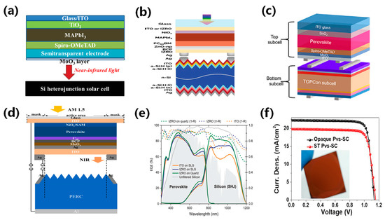
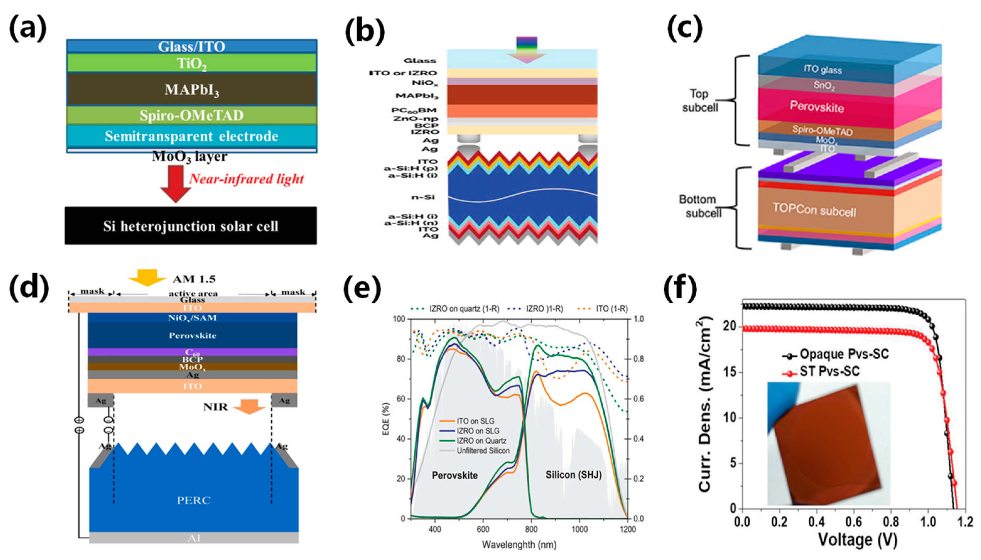
Figure 9.
Schematics of 4T PVK/Si tandem architectures: (a) NIP structured PVK top cell/SHJ bottom cell [70]. Reproduced with permission: Copyright 2019, John Wiley and Sons. (b) PIN structured PVK entire cell/SHJ bottom cell [95]. Reproduced with permission: Copyright 2019, John Wiley and Sons. (c) NIP structured PVK entire cell/TOPCon bottom cell [80]. Reproduced with permission: Copyright 2023, Elsevier Inc. (d) PIN structured PVK entire cell/PERC bottom cell [96]. Reproduced with permission: Copyright 2023, Elsevier B.V. (e) EQE spectra of a NIP structured PVK/Si tandem cell [95]. Reproduced with permission: Copyright 2019, John Wiley and Sons. (f) The J-V characteristics of ST-PVK and opaque PVK solar cells [70]. Reproduced with permission: Copyright 2019, John Wiley and Sons.
PERC, IBC, and TOPCon solar cells are commonly used as bottom cells in 4T perovskite/Si tandem solar cells. PERC solar cells passivate the rear contact and could reduce reflection and surface recombination, resulting in improved efficiency and lower production costs. IBC solar cells minimize front surface electron shading to enhance efficiency and result in higher manufacturing costs. The TOPCon solar cell introduced a micrometer-scale tunnel oxide passivation layer in the contact area to reduce electron-hole recombination, thereby improving the open-circuit voltage and fill factor. However, the preparation process and material costs of the TOPCon solar cell are much higher than other Si cells. Duong et al. [97] meticulously explored electrical and optical power losses across cells, resulting in an NIP-structured PVK top cell utilizing an ITO electrode with over 80% infrared transparency. Perovskite/Si tandem solar cells based on PERL cells have achieved an efficiency of 20.1% due to their better light absorption properties. Duong et al. [86] synthesized an innovative PVK top cell and reduced surface defects by introducing MABr surface passivation. They further combined this with a PERL cell to fabricate a 4T perovskite/Si tandem solar cell with an efficiency of 26.2%. Mehedad et al. [98] fabricated a 4T perovskite/Si tandem solar cell with an intruding ZnO buffer layer and combined it with the PERT cell, resulting in an efficiency of 21.1%, as shown in Figure 10e. Manoj et al. [74] applied optical simulation to devise a 4T perovskite/Si tandem solar cell structure which minimizes light leakage on both textured and flat Si surfaces. The perovskite/Si tandem solar cells based on the IBC bottom cell achieved an efficiency of 25.5%. Manoj et al. [85] introduced an innovative approach by placing an ALD-processed Al2O3 passivation layer between the PVK layer (Cs0.15(CH5NH2)0.85Pb(I0.71Br0.29)3) and the spiro HTL to successfully reduce the nonradiative recombination, resulting in a high Voc of 1.22 V. The 4T perovskite/Si tandem cell with an Al2O3 passivation layer and IBC bottom cell yielded efficiencies of 27.1% (0.13 cm2) and 25.3% (4 cm2). Zhang et al. [78] fabricated the 4T perovskite/Si tandem solar cells based on the IBC cell and achieved an efficiency of 25.7% with a near-infrared transmittance of 92%. Chai et al. [82] used Pb(SCN)2 and MACl additives to improve high film quality. They found that the introduction of Pb(SCN)2 could improve crystallinity and generate excess PbI2, while the introduction of MACl could react with the excess PbI2 to create MAPbI3−xClx. The 4T perovskite/TOPCon silicon tandem device achieved an impressive efficiency of 30.91% and excellent stability. Ajeet et al. [79] conceived a TOPCon sub-cell and stacked a Cs0.05FA0.8MA0.15PbI2.55Br0.45 PVK top cell, engineering a 4T PVK/Si tandem solar cell that delivered 26.7% efficiency. Recently, Wu et al. [76] proposed a method to reconstruct the ITO surface using an HF and subsequent UVO treatment. This method selectively removes undesired terminal hydroxyls and hydrolysis products, enhancing SAM adsorption and preventing direct contact with the perovskite layer. The 4T perovskite/Si tandem solar cell obtained an efficiency of 28.4%. A summary of 4T perovskite /Si tandem solar cells is presented in Table 2.
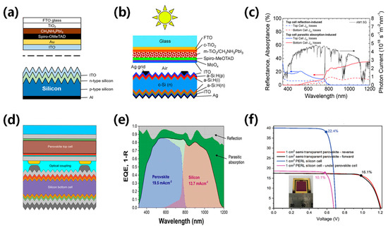

Figure 10.
(a) Structural image of the top cell: NIP structured PVK solar cell and bottom cell [99]. Reproduced with permission: Copyright 2018, American Chemical Society. (b) Schematic of the mechanically stacked four-terminal tandem and (c) current loss spectra separated into the top cell and bottom cell current losses [94]. Copyright 1999, Royal Society of Chemistry (Great Britain). (d) Structural image of NIP structured PVK top cell/SHJ bottom cell [93]. Reproduced with permission: Copyright 2016, American Chemical Society. (e) EQE of PVK solar cells by atmospheric pressure spatial atomic layer deposited ZnO [98]. Reproduced with permission: Copyright 2018, John Wiley and Sons. (f) Corresponding certified J–V data (1 cm2 aperture area) [86]. Reproduced with permission: Copyright 2020, John Wiley and Sons.
Table 2.
Summary of 4T PVK/Si tandem solar cells.
7. Conclusions and Outlook
This review summarized recent progress in the development of ST-PSCs and 4T-PVK/Si tandem solar cells. It highlights the effects of the translucent structure mechanism, transparent electrodes, charge transport layer, and perovskite component modification in semitransparent perovskite solar cells. Furthermore, we discussed the application of semitransparent perovskite solar cells in perovskite/Si tandem solar cells. However, there is significant room to further develop the efficiency of 4T perovskite/Si tandem solar cells.
The development and application of ST-PSCs have received unprecedented attention against the current low carbon and green energy backdrop. However, it is necessary to further develop the efficiency of ST-PSCs. The main challenge is to balance the light transmittance and perovskite film thickness. One effective strategy to increase current density and efficiency of ST-PSCs is to fabricate thicker film, which will absorb more light in the top cell. The high efficiency and high transmittance of ST-PSCs will further promote the development of 4T perovskite/Si tandem solar cells.
Perovskite light-absorbing layers with optically active microstructures or nanostructures may be frequently employed to improve device performance. It is important to prepare a buffer layer to prevent AgNWs reactions that could lead to a degradation in device performance. More importantly, the main challenge for transparent electrodes is to balance high conductivity and high transmittance. Additionally, the stability of ultra-thin metals need to be further considered and can be improved by developing DMD structures. It is necessary to develop novel structures to optimize transmittance without compromising on performance. Transparent conductive materials with high mobility could improve the light capture capacity of the device, and an anti-reflection layer or light management foil could further promote the development of the perovskite/Si tandem solar cell. Regarding the charge transport layer, it is important to investigate new materials with favorable energy level alignment, high transparency, and high conductivity.
To further develop 4T Perovskite/Si tandem solar cells, it is essential to enhance their efficiency and reduce their fabrication cost. Thus, it is necessary to develop large-scale perovskite deposition processes. In recent years, spin-coating has been widely used in the fabrication of tandem solar cells to achieve high tandem efficiency. The spin-coated method enables the formation of high-quality perovskite films with optimized thickness and bandgap. However, the spin-coated method is not suitable for large-scale processes. Large-scale perovskite solar cells are typically produced using techniques such as evaporation, spray coating, slot-dye coating, and blade coating. It is a challenge to fabricate large area ST-PSCs with high efficiency and high transmittance.
Despite the existence of these challenges, it is expected that researchers will continue to develop more promising strategies to overcome them. Given ongoing improvements in ST-PSCs and Si solar cells, it is believed that 4T perovskite/Si tandem solar cells will play an increasingly indispensable role in solar energy and clean energy development.
Author Contributions
This work was conceived by Y.Z., L.Z. and C.Z. All authors have read and agreed to the published version of the manuscript.
Funding
This work was financially supported by the National Natural Science Foundation of China (62204189, 62274126), the National Key R&D Program of China (2021YFF0500504, 2021YFF0500501), the Natural Science Basic Research Plan in Shaanxi Province of China (2024GX-YBXM-514), the Fundamental Research Funds for the Central Universities, and the Young Talent Fund of Association for Science and Technology in Shaanxi, China (20220115).
Data Availability Statement
Data are available upon request.
Conflicts of Interest
L.Z. and C.Z. were employed by Xi’an Baoxin Solar Technology Co., Ltd. The remaining authors declare that the research was conducted in the absence of any commercial or financial relationships that could be construed as a potential conflict of interest.
References
- Lal, N.N.; Dkhissi, Y.; Li, W.; Hou, Q.; Cheng, Y.; Bach, U. Perovskite Tandem Solar Cells. Adv. Energy Mater. 2017, 7, 1602761. [Google Scholar] [CrossRef]
- Ito, K.; Nonomura, K.; Kan, R.; Tada, K.; Lin, C.C.; Kinoshita, T.; Bessho, T.; Uchida, S.; Segawa, H. Spectral Splitting Solar Cells Consisting of a Mesoscopic Wide-Bandgap Perovskite Solar Cell and an Inverted Narrow-Bandgap Perovskite Solar Cell. ACS Omega 2024, 9, 3028–3034. [Google Scholar] [CrossRef] [PubMed]
- Lin, C.-F.; Lin, T.-F.; Li, M.-H.; Lin, P.-Y.; Raifuku, I.; Hsieh, P.-T.; Chen, P. Back-Contact Perovskite Solar Cells. Semicond. Sci. Technol. 2021, 36, 83001. [Google Scholar] [CrossRef]
- Rahmany, S.; Etgar, L. Semitransparent Perovskite Solar Cells. ACS Energy Lett. 2020, 5, 1519–1531. [Google Scholar] [CrossRef]
- Wang, D.; Wright, M.; Elumalai, N.K.; Uddin, A. Stability of Perovskite Solar Cells. Sol. Energy Mater. Sol. Cells 2016, 147, 255–275. [Google Scholar] [CrossRef]
- De Wolf, S.; Holovsky, J.; Moon, S.-J.; Löper, P.; Niesen, B.; Ledinsky, M.; Haug, F.-J.; Yum, J.-H.; Ballif, C. Organometallic Halide Perovskites: Sharp Optical Absorption Edge and Its Relation to Photovoltaic Performance. J. Phys. Chem. Lett. 2014, 5, 1035–1039. [Google Scholar] [CrossRef]
- Savenije, T.J.; Ponseca, C.S.; Kunneman, L.; Abdellah, M.; Zheng, K.; Tian, Y.; Zhu, Q.; Canton, S.E.; Scheblykin, I.G.; Pullerits, T.; et al. Thermally Activated Exciton Dissociation and Recombination Control the Carrier Dynamics in Organometal Halide Perovskite. J. Phys. Chem. Lett. 2014, 5, 2189–2194. [Google Scholar] [CrossRef] [PubMed]
- Stranks, S.D.; Eperon, G.E.; Grancini, G.; Menelaou, C.; Alcocer, M.J.P.; Leijtens, T.; Herz, L.M.; Petrozza, A.; Snaith, H.J. Electron-Hole Diffusion Lengths Exceeding 1 Micrometer in an Organometal Trihalide Perovskite Absorber. Science 2013, 342, 341–344. [Google Scholar] [CrossRef] [PubMed]
- Kulkarni, S.A.; Baikie, T.; Boix, P.P.; Yantara, N.; Mathews, N.; Mhaisalkar, S. Band-Gap Tuning of Lead Halide Perovskites Using a Sequential Deposition Process. J. Mater. Chem. A 2014, 2, 9221–9225. [Google Scholar] [CrossRef]
- Binetti, S.; Acciarri, M.; Le Donne, A.; Morgano, M.; Jestin, Y. Key Success Factors and Future Perspective of Silicon-Based Solar Cells. Int. J. Photoenergy 2013, 2013, 249502. [Google Scholar] [CrossRef]
- Andreani, L.C.; Bozzola, A.; Kowalczewski, P.; Liscidini, M.; Redorici, L. Silicon Solar Cells: Toward the Efficiency Limits. Adv. Phys. X 2019, 4, 1548305. [Google Scholar] [CrossRef]
- Liang, Z.; Zhang, Y.; Xu, H.; Chen, W.; Liu, B.; Zhang, J.; Zhang, H.; Wang, Z.; Kang, D.-H.; Zeng, J.; et al. Homogenizing Out-of-Plane Cation Composition in Perovskite Solar Cells. Nature 2023, 624, 557–563. [Google Scholar] [CrossRef] [PubMed]
- Geisz, J.F.; France, R.M.; Schulte, K.L.; Steiner, M.A.; Norman, A.G.; Guthrey, H.L.; Young, M.R.; Song, T.; Moriarty, T. Six-Junction III–V Solar Cells with 47.1% Conversion Efficiency under 143 Suns Concentration. Nat. Energy 2020, 5, 326–335. [Google Scholar] [CrossRef]
- Jošt, M.; Kegelmann, L.; Korte, L.; Albrecht, S. Monolithic Perovskite Tandem Solar Cells: A Review of the Present Status and Advanced Characterization Methods Toward 30% Efficiency. Adv. Energy Mater. 2020, 10, 1904102. [Google Scholar] [CrossRef]
- Chen, Q.; Zhou, L.; Zhang, J.; Chen, D.; Zhu, W.; Xi, H.; Zhang, J.; Zhang, C.; Hao, Y. Recent Progress of Wide Bandgap Perovskites towards Two-Terminal Perovskite/Silicon Tandem Solar Cells. Nanomaterials 2024, 14, 202. [Google Scholar] [CrossRef] [PubMed]
- Fu, F.; Li, J.; Yang, T.C.; Liang, H.; Faes, A.; Jeangros, Q.; Ballif, C.; Hou, Y. Monolithic Perovskite-Silicon Tandem Solar Cells: From the Lab to Fab? Adv. Mater. 2022, 34, 2106540. [Google Scholar] [CrossRef] [PubMed]
- Coletti, G.; Luxembourg, S.L.; Geerligs, L.J.; Rosca, V.; Burgers, A.R.; Wu, Y.; Okel, L.; Kloos, M.; Danzl, F.J.K.; Najafi, M.; et al. Bifacial Four-Terminal Perovskite/Silicon Tandem Solar Cells and Modules. ACS Energy Lett. 2020, 5, 1676–1680. [Google Scholar] [CrossRef]
- Kothandaraman, R.K.; Jiang, Y.; Feurer, T.; Tiwari, A.N.; Fu, F. Near-Infrared-Transparent Perovskite Solar Cells and Perovskite-Based Tandem Photovoltaics. Small Methods 2020, 4, 2000395. [Google Scholar] [CrossRef]
- Leijtens, T.; Bush, K.A.; Prasanna, R.; McGehee, M.D. Opportunities and Challenges for Tandem Solar Cells Using Metal Halide Perovskite Semiconductors. Nat. Energy 2018, 3, 828–838. [Google Scholar] [CrossRef]
- Kim, C.U.; Jung, E.D.; Noh, Y.W.; Seo, S.K.; Choi, Y.; Park, H.; Song, M.H.; Choi, K.J. Strategy for large-scale Monolithic Perovskite/Silicon Tandem Solar Cell: A Review of Recent Progress. EcoMat 2021, 3, e12084. [Google Scholar] [CrossRef]
- Wang, Z.; Song, Z.; Yan, Y.; Liu, S.; Yang, D. Perovskite—A Perfect Top Cell for Tandem Devices to Break the S–Q Limit. Adv. Sci. 2019, 6, 1801704. [Google Scholar] [CrossRef]
- Walsh, A. Principles of Chemical Bonding and Band Gap Engineering in Hybrid Organic–Inorganic Halide Perovskites. J. Phys. Chem. C 2015, 119, 5755–5760. [Google Scholar] [CrossRef] [PubMed]
- Yuan, L.; Wang, Z.; Duan, R.; Huang, P.; Zhang, K.; Chen, Q.; Allam, N.K.; Zhou, Y.; Song, B.; Li, Y. Semi-Transparent Perovskite Solar Cells: Unveiling the Trade-off between Transparency and Efficiency. J. Mater. Chem. A 2018, 6, 19696–19702. [Google Scholar] [CrossRef]
- Ball, J.M.; Stranks, S.D.; Hörantner, M.T.; Hüttner, S.; Zhang, W.; Crossland, E.J.W.; Ramirez, I.; Riede, M.; Johnston, M.B.; Friend, R.H.; et al. Optical Properties and Limiting Photocurrent of Thin-Film Perovskite Solar Cells. Energy Environ. Sci. 2015, 8, 602–609. [Google Scholar] [CrossRef]
- Ramírez Quiroz, C.O.; Levchuk, I.; Bronnbauer, C.; Salvador, M.; Forberich, K.; Heumüller, T.; Hou, Y.; Schweizer, P.; Spiecker, E.; Brabec, C.J. Pushing Efficiency Limits for Semitransparent Perovskite Solar Cells. J. Mater. Chem. A 2015, 3, 24071–24081. [Google Scholar] [CrossRef]
- Roldán-Carmona, C.; Malinkiewicz, O.; Betancur, R.; Longo, G.; Momblona, C.; Jaramillo, F.; Camacho, L.; Bolink, H.J. High Efficiency Single-Junction Semitransparent Perovskite Solar Cells. Energy Environ. Sci. 2014, 7, 2968–2973. [Google Scholar] [CrossRef]
- Chen, W.; Zhang, J.; Xu, G.; Xue, R.; Li, Y.; Zhou, Y.; Hou, J.; Li, Y. A Semitransparent Inorganic Perovskite Film for Overcoming Ultraviolet Light Instability of Organic Solar Cells and Achieving 14.03% Efficiency. Adv. Mater. 2018, 30, 1800855. [Google Scholar] [CrossRef] [PubMed]
- Bag, S.; Durstock, M.F. Efficient Semi-Transparent Planar Perovskite Solar Cells Using a ‘Molecular Glue’. Nano Energy 2016, 30, 542–548. [Google Scholar] [CrossRef]
- Guo, Y.; Shoyama, K.; Sato, W.; Nakamura, E. Polymer Stabilization of Lead(II) Perovskite Cubic Nanocrystals for Semitransparent Solar Cells. Adv. Energy Mater. 2016, 6, 1502317. [Google Scholar] [CrossRef]
- Wen, Q.; Duan, C.; Zou, F.; Luo, D.; Li, J.; Liu, Z.; Wang, J.; Yan, K. All-Inorganic CsPb1-XSnxI2Br Perovskites Mediated by Dicyandiamide Additive for Efficient 4-Terminal Tandem Solar Cell. Chem. Eng. J. 2023, 452, 139697. [Google Scholar] [CrossRef]
- Ponchai, J.; Kaewurai, P.; Boonthum, C.; Pinsuwan, K.; Supasai, T.; Sahasithiwat, S.; Kanjanaboos, P. Modifying Morphology and Defects of Low-Dimensional, Semi-Transparent Perovskite Thin Films via Solvent Type. RSC Adv. 2019, 9, 12047–12054. [Google Scholar] [CrossRef] [PubMed]
- Yao, Y.; Hang, P.; Li, B.; Hu, Z.; Kan, C.; Xie, J.; Wang, Y.; Zhang, Y.; Yang, D.; Yu, X. Phase-Stable Wide-Bandgap Perovskites for Four-Terminal Perovskite/Silicon Tandem Solar Cells with Over 30% Efficiency. Small 2022, 18, 2203319. [Google Scholar] [CrossRef] [PubMed]
- Zhang, Z.; Ji, R.; Jia, X.; Wang, S.; Deconinck, M.; Siliavka, E.; Vaynzof, Y. Semitransparent Perovskite Solar Cells with an Evaporated Ultra-Thin Perovskite Absorber. Adv. Funct. Mater. 2023, 2307471. [Google Scholar] [CrossRef]
- Eperon, G.E.; Burlakov, V.M.; Goriely, A.; Snaith, H.J. Neutral Color Semitransparent Microstructured Perovskite Solar Cells. ACS Nano 2014, 8, 591–598. [Google Scholar] [CrossRef] [PubMed]
- Chen, S.; Chen, B.; Gao, X.; Dong, B.; Hu, H.; Yan, K.; Wen, W.; Zou, D. Neutral-Colored Semitransparent Solar Cells Based on Pseudohalide (SCN − )-Doped Perovskite. Sustain. Energy Fuels 2017, 1, 1034–1040. [Google Scholar] [CrossRef]
- Hörantner, M.T.; Nayak, P.K.; Mukhopadhyay, S.; Wojciechowski, K.; Beck, C.; McMeekin, D.; Kamino, B.; Eperon, G.E.; Snaith, H.J. Shunt-Blocking Layers for Semitransparent Perovskite Solar Cells. Adv. Mater. Interfaces 2016, 3, 1500837. [Google Scholar] [CrossRef]
- Aharon, S.; Layani, M.; Cohen, B.; Shukrun, E.; Magdassi, S.; Etgar, L. Self-Assembly of Perovskite for Fabrication of Semitransparent Perovskite Solar Cells. Adv. Mater. Interfaces 2015, 2, 1500118. [Google Scholar] [CrossRef]
- Rahmany, S.; Layani, M.; Magdassi, S.; Etgar, L. Fully Functional Semi-Transparent Perovskite Solar Cell Fabricated in Ambient Air. Sustain. Energy Fuels 2017, 1, 2120–2127. [Google Scholar] [CrossRef]
- Rai, M.; Rahmany, S.; Lim, S.S.; Magdassi, S.; Wong, L.H.; Etgar, L. Hot Dipping Post Treatment for Improved Efficiency in Micro Patterned Semi-Transparent Perovskite Solar Cells. J. Mater. Chem. A 2018, 6, 23787–23796. [Google Scholar] [CrossRef]
- Kim, G.M.; Tatsuma, T. Semitransparent Solar Cells with Ultrasmooth and Low-Scattering Perovskite Thin Films. J. Phys. Chem. C 2016, 120, 28933–28938. [Google Scholar] [CrossRef]
- Bailie, C.D.; Christoforo, M.G.; Mailoa, J.P.; Bowring, A.R.; Unger, E.L.; Nguyen, W.H.; Burschka, J.; Pellet, N.; Lee, J.Z.; Grätzel, M.; et al. Semi-Transparent Perovskite Solar Cells for Tandems with Silicon and CIGS. Energy Environ. Sci. 2015, 8, 956–963. [Google Scholar] [CrossRef]
- Guchhait, A.; Dewi, H.A.; Leow, S.W.; Wang, H.; Han, G.; Suhaimi, F.B.; Mhaisalkar, S.; Wong, L.H.; Mathews, N. Over 20% Efficient CIGS–Perovskite Tandem Solar Cells. ACS Energy Lett. 2017, 2, 807–812. [Google Scholar] [CrossRef]
- Fu, F.; Feurer, T.; Jäger, T.; Avancini, E.; Bissig, B.; Yoon, S.; Buecheler, S.; Tiwari, A.N. Low-Temperature-Processed Efficient Semi-Transparent Planar Perovskite Solar Cells for Bifacial and Tandem Applications. Nat. Commun. 2015, 6, 8932. [Google Scholar] [CrossRef] [PubMed]
- Bid, A.; Bora, A.; Raychaudhuri, A.K. Publisher’s Note: Temperature Dependence of the Resistance of Metallic Nanowires of Diameter ≥ 15 nm: Applicability of Bloch-Grüneisen Theorem. Phys. Rev. B 2006, 74, 79903. [Google Scholar] [CrossRef]
- Guo, F.; Azimi, H.; Hou, Y.; Przybilla, T.; Hu, M.; Bronnbauer, C.; Langner, S.; Spiecker, E.; Forberich, K.; Brabec, C.J. High-Performance Semitransparent Perovskite Solar Cells with Solution-Processed Silver Nanowires as Top Electrodes. Nanoscale 2015, 7, 1642–1649. [Google Scholar] [CrossRef]
- Chang, C.-Y.; Lee, K.-T.; Huang, W.-K.; Siao, H.-Y.; Chang, Y.-C. High-Performance, Air-Stable, Low-Temperature Processed Semitransparent Perovskite Solar Cells Enabled by Atomic Layer Deposition. Chem. Mater. 2015, 27, 5122–5130. [Google Scholar] [CrossRef]
- Li, Z.; Kulkarni, S.A.; Boix, P.P.; Shi, E.; Cao, A.; Fu, K.; Batabyal, S.K.; Zhang, J.; Xiong, Q.; Wong, L.H.; et al. Laminated Carbon Nanotube Networks for Metal Electrode-Free Efficient Perovskite Solar Cells. ACS Nano 2014, 8, 6797–6804. [Google Scholar] [CrossRef]
- Li, F.R.; Xu, Y.; Chen, W.; Xie, S.H.; Li, J.Y. Nanotube Enhanced Carbon Grids as Top Electrodes for Fully Printable Mesoscopic Semitransparent Perovskite Solar Cells. J. Mater. Chem. A 2017, 5, 10374–10379. [Google Scholar] [CrossRef]
- Tai, Q.; Yan, F. Emerging Semitransparent Solar Cells: Materials and Device Design. Adv. Mater. 2017, 29, 1700192. [Google Scholar] [CrossRef] [PubMed]
- Bouville, F.; Maire, E.; Meille, S.; Van de Moortèle, B.; Stevenson, A.J.; Deville, S. Strong, Tough and Stiff Bioinspired Ceramics from Brittle Constituents. Nat. Mater. 2014, 13, 508–514. [Google Scholar] [CrossRef] [PubMed]
- You, P.; Liu, Z.; Tai, Q.; Liu, S.; Yan, F. Efficient Semitransparent Perovskite Solar Cells with Graphene Electrodes. Adv. Mater. 2015, 27, 3632–3638. [Google Scholar] [CrossRef]
- Lee, H.-J.; Cho, S.-P.; Na, S.; Kim, S.-S. Thin Metal Top Electrode and Interface Engineering for Efficient and Air-Stable Semitransparent Perovskite Solar Cells. J. Alloys Compd. 2019, 797, 65–73. [Google Scholar] [CrossRef]
- Ying, Z.; Chen, W.; Lin, Y.; He, Z.; Chen, T.; Zhu, Y.; Zhang, X.; Yang, X.; Djurišić, A.B.; He, Z. Supersmooth Ta2O5/Ag/Polyetherimide Film as the Rear Transparent Electrode for High Performance Semitransparent Perovskite Solar Cells. Adv. Opt. Mater. 2019, 7, 1801409. [Google Scholar] [CrossRef]
- Chen, D.; Pang, S.; Zhou, L.; Li, X.; Su, A.; Zhu, W.; Chang, J.; Zhang, J.; Zhang, C.; Hao, Y. An Efficient TeO2/Ag Transparent Top Electrode for 20%-Efficiency Bifacial Perovskite Solar Cells with a Bifaciality Factor Exceeding 80%. J. Mater. Chem. A 2019, 7, 15156–15163. [Google Scholar] [CrossRef]
- Della Gaspera, E.; Peng, Y.; Hou, Q.; Spiccia, L.; Bach, U.; Jasieniak, J.J.; Cheng, Y.-B. Ultra-Thin High Efficiency Semitransparent Perovskite Solar Cells. Nano Energy 2015, 13, 249–257. [Google Scholar] [CrossRef]
- Yang, Y.; Chen, Q.; Hsieh, Y.-T.; Song, T.-B.; De Marco, N.; Zhou, H.; Yang, Y. Multilayer Transparent Top Electrode for Solution Processed Perovskite/Cu(In,Ga)(Se,S)2 Four Terminal Tandem Solar Cells. ACS Nano 2015, 9, 7714–7721. [Google Scholar] [CrossRef]
- Bu, L.; Liu, Z.; Zhang, M.; Li, W.; Zhu, A.; Cai, F.; Zhao, Z.; Zhou, Y. Semitransparent Fully Air Processed Perovskite Solar Cells. ACS Appl. Mater. Interfaces 2015, 7, 17776–17781. [Google Scholar] [CrossRef]
- Heo, J.H.; Han, H.J.; Lee, M.; Song, M.; Kim, D.H.; Im, S.H. Stable Semi-Transparent CH3NH3PbI3 Planar Sandwich Solar Cells. Energy Environ. Sci. 2015, 8, 2922–2927. [Google Scholar] [CrossRef]
- Bush, K.A.; Bailie, C.D.; Chen, Y.; Bowring, A.R.; Wang, W.; Ma, W.; Leijtens, T.; Moghadam, F.; McGehee, M.D. Thermal and Environmental Stability of Semi-Transparent Perovskite Solar Cells for Tandems Enabled by a Solution-Processed Nanoparticle Buffer Layer and Sputtered ITO Electrode. Adv. Mater. 2016, 28, 3937–3943. [Google Scholar] [CrossRef]
- Werner, J.; Dubuis, G.; Walter, A.; Löper, P.; Moon, S.-J.; Nicolay, S.; Morales-Masis, M.; De Wolf, S.; Niesen, B.; Ballif, C. Sputtered Rear Electrode with Broadband Transparency for Perovskite Solar Cells. Sol. Energy Mater. Sol. Cells 2015, 141, 407–413. [Google Scholar] [CrossRef]
- Meng, L.; You, J.; Guo, T.-F.; Yang, Y. Recent Advances in the Inverted Planar Structure of Perovskite Solar Cells. Acc. Chem. Res. 2016, 49, 155–165. [Google Scholar] [CrossRef] [PubMed]
- Sun, K.; Li, P.; Xia, Y.; Chang, J.; Ouyang, J. Transparent Conductive Oxide-Free Perovskite Solar Cells with PEDOT:PSS as Transparent Electrode. ACS Appl. Mater. Interfaces 2015, 7, 15314–15320. [Google Scholar] [CrossRef] [PubMed]
- Lee, K.-T.; Guo, L.; Park, H. Neutral- and Multi-Colored Semitransparent Perovskite Solar Cells. Molecules 2016, 21, 475. [Google Scholar] [CrossRef] [PubMed]
- Boccard, M.; Rodkey, N.; Holman, Z.C. High-Mobility Hydrogenated Indium Oxide without Introducing Water During Sputtering. Energy Procedia 2016, 92, 297–303. [Google Scholar] [CrossRef]
- Werner, J.; Weng, C.-H.; Walter, A.; Fesquet, L.; Seif, J.P.; De Wolf, S.; Niesen, B.; Ballif, C. Efficient Monolithic Perovskite/Silicon Tandem Solar Cell with Cell Area > 1 cm2. J. Phys. Chem. Lett. 2016, 7, 161–166. [Google Scholar] [CrossRef] [PubMed]
- Wahl, T.; Hanisch, J.; Meier, S.; Schultes, M.; Ahlswede, E. Sputtered Indium Zinc Oxide Rear Electrodes for Inverted Semitransparent Perovskite Solar Cells without Using a Protective Buffer Layer. Org. Electron. 2018, 54, 48–53. [Google Scholar] [CrossRef]
- Fu, F.; Feurer, T.; Weiss, T.P.; Pisoni, S.; Avancini, E.; Andres, C.; Buecheler, S.; Tiwari, A.N. High-Efficiency Inverted Semi-Transparent Planar Perovskite Solar Cells in Substrate Configuration. Nat. Energy 2016, 2, 16190. [Google Scholar] [CrossRef]
- Yoon, S.; Ha, H.U.; Seok, H.; Kim, H.; Kang, D. Highly Efficient and Reliable Semitransparent Perovskite Solar Cells via Top Electrode Engineering. Adv. Funct. Mater. 2022, 32, 2111760. [Google Scholar] [CrossRef]
- Naqvi, S.D.H.; Son, K.; Jung, W.; Hwang, H.U.; Lee, S.; Lee, A.; Keum, M.; Kim, S.; Kim, J.W.; Kang, M.G.; et al. Mitigating Intrinsic Interfacial Degradation in Semi-Transparent Perovskite Solar Cells for High Efficiency and Long-Term Stability. Adv. Energy Mater. 2023, 13, 2302147. [Google Scholar] [CrossRef]
- Wang, Z.; Zhu, X.; Zuo, S.; Chen, M.; Zhang, C.; Wang, C.; Ren, X.; Yang, Z.; Liu, Z.; Xu, X.; et al. 27%-Efficiency Four-Terminal Perovskite/Silicon Tandem Solar Cells by Sandwiched Gold Nanomesh. Adv. Funct. Mater. 2020, 30, 1908298. [Google Scholar] [CrossRef]
- Duong, T.; Nguyen, T.; Huang, K.; Pham, H.; Adhikari, S.G.; Khan, M.R.; Duan, L.; Liang, W.; Fong, K.C.; Shen, H.; et al. Bulk Incorporation with 4-Methylphenethylammonium Chloride for Efficient and Stable Methylammonium-Free Perovskite and Perovskite-Silicon Tandem Solar Cells. Adv. Energy Mater. 2023, 13, 2203607. [Google Scholar] [CrossRef]
- Sun, J.; Zhang, N.; Wu, J.; Yang, W.; He, H.; Huang, M.; Zeng, Y.; Yang, X.; Ying, Z.; Qin, G.; et al. Additive Engineering of the CuSCN Hole Transport Layer for High-Performance Perovskite Semitransparent Solar Cells. ACS Appl. Mater. Interfaces 2022, 14, 52223–52232. [Google Scholar] [CrossRef] [PubMed]
- Jeong, M.J.; Lee, J.H.; You, C.H.; Kim, S.Y.; Lee, S.; Noh, J.H. Oxide/Halide/Oxide Architecture for High Performance Semi-Transparent Perovskite Solar Cells. Adv. Energy Mater. 2022, 12, 2200661. [Google Scholar] [CrossRef]
- Jaysankar, M.; Filipič, M.; Zielinski, B.; Schmager, R.; Song, W.; Qiu, W.; Paetzold, U.W.; Aernouts, T.; Debucquoy, M.; Gehlhaar, R.; et al. Perovskite–Silicon Tandem Solar Modules with Optimised Light Harvesting. Energy Environ. Sci. 2018, 11, 1489–1498. [Google Scholar] [CrossRef]
- Dewi, H.A.; Wang, H.; Li, J.; Thway, M.; Sridharan, R.; Stangl, R.; Lin, F.; Aberle, A.G.; Mathews, N.; Bruno, A.; et al. Highly Efficient Semitransparent Perovskite Solar Cells for Four Terminal Perovskite-Silicon Tandems. ACS Appl. Mater. Interfaces 2019, 11, 34178–34187. [Google Scholar] [CrossRef]
- Wu, M.; Li, X.; Ying, Z.; Chen, Y.; Wang, X.; Zhang, M.; Su, S.; Guo, X.; Sun, J.; Shou, C.; et al. Reconstruction of the Indium Tin Oxide Surface Enhances the Adsorption of High-Density Self-Assembled Monolayer for Perovskite/Silicon Tandem Solar Cells. Adv. Funct. Mater. 2023, 33, 2304708. [Google Scholar] [CrossRef]
- Gharibzadeh, S.; Hossain, I.M.; Fassl, P.; Nejand, B.A.; Abzieher, T.; Schultes, M.; Ahlswede, E.; Jackson, P.; Powalla, M.; Schäfer, S.; et al. 2D/3D Heterostructure for Semitransparent Perovskite Solar Cells with Engineered Bandgap Enables Efficiencies Exceeding 25% in Four-Terminal Tandems with Silicon and CIGS. Adv. Funct. Mater. 2020, 30, 1909919. [Google Scholar] [CrossRef]
- Zhang, D.; Najafi, M.; Zardetto, V.; Dörenkämper, M.; Zhou, X.; Veenstra, S.; Geerligs, L.J.; Aernouts, T.; Andriessen, R. High Efficiency 4-Terminal Perovskite/c-Si Tandem Cells. Sol. Energy Mater. Sol. Cells 2018, 188, 1–5. [Google Scholar] [CrossRef]
- Rohatgi, A.; Zhu, K.; Tong, J.; Kim, D.H.; Reichmanis, E.; Rounsaville, B.; Prakash, V.; Ok, Y.-W. 26.7% Efficient 4-Terminal Perovskite–Silicon Tandem Solar Cell Composed of a High-Performance Semitransparent Perovskite Cell and a Doped Poly-Si/SiOx Passivating Contact Silicon Cell. IEEE J. Photovolt. 2020, 10, 417–422. [Google Scholar] [CrossRef]
- Li, Z.; Li, X.; Chen, X.; Cui, X.; Guo, C.; Feng, X.; Ren, D.; Mo, Y.; Yang, M.; Huang, H.; et al. In Situ Epitaxial Growth of Blocking Structure in Mixed-Halide Wide-Band-Gap Perovskites for Efficient Photovoltaics. Joule 2023, 7, 1363–1381. [Google Scholar] [CrossRef]
- Tao, J.; Liu, X.; Shen, J.; Han, S.; Guan, L.; Fu, G.; Kuang, D.-B.; Yang, S. F-Type Pseudo-Halide Anions for High-Efficiency and Stable Wide-Band-Gap Inverted Perovskite Solar Cells with Fill Factor Exceeding 84%. ACS Nano 2022, 16, 10798–10810. [Google Scholar] [CrossRef] [PubMed]
- Chai, W.; Li, L.; Zhu, W.; Chen, D.; Zhou, L.; Xi, H.; Zhang, J.; Zhang, C.; Hao, Y. Graded Heterojunction Improves Wide-Bandgap Perovskite for Highly Efficient 4-Terminal Perovskite/Silicon Tandem Solar Cells. Research 2023, 6, 196. [Google Scholar] [CrossRef]
- Tao, J.; Xue, J.; Guo, H.; Wang, Y.; Shen, J.; Wang, T.; He, T.; Fu, G.; Yang, S. Precisely Adjusting the Organic/Electrode Interface Charge Barrier for Efficient and Stable Ag-Based Regular Perovskite Solar Cells with >23% Efficiency. Chem. Eng. J. 2023, 463, 142445. [Google Scholar] [CrossRef]
- Yu, B.; Tang, F.; Yang, Y.; Huang, J.; Wu, S.; Lu, F.; Duan, W.; Lambertz, A.; Ding, K.; Mai, Y. Impermeable Atomic Layer Deposition for Sputtering Buffer Layer in Efficient Semi-Transparent and Tandem Solar Cells via Activating Unreactive Substrate. Adv. Mater. 2023, 35, 2202447. [Google Scholar] [CrossRef] [PubMed]
- Jaysankar, M.; Raul, B.A.L.; Bastos, J.; Burgess, C.; Weijtens, C.; Creatore, M.; Aernouts, T.; Kuang, Y.; Gehlhaar, R.; Hadipour, A.; et al. Minimizing Voltage Loss in Wide-Bandgap Perovskites for Tandem Solar Cells. ACS Energy Lett. 2019, 4, 259–264. [Google Scholar] [CrossRef]
- Duong, T.; Pham, H.; Kho, T.C.; Phang, P.; Fong, K.C.; Yan, D.; Yin, Y.; Peng, J.; Mahmud, M.A.; Gharibzadeh, S.; et al. High Efficiency Perovskite-Silicon Tandem Solar Cells: Effect of Surface Coating versus Bulk Incorporation of 2D Perovskite. Adv. Energy Mater. 2020, 10, 1903553. [Google Scholar] [CrossRef]
- Tian, C.; Gao, X.; Li, J.; Pan, J.; Yu, G.; Huang, B.; Wen, Y.; Zhu, H.; Bu, T.; Cheng, Y.-B.; et al. Scalable Growth of Stable Wide-Bandgap Perovskite towards Large-Scale Tandem Photovoltaics. Sol. RRL 2022, 6, 2200134. [Google Scholar] [CrossRef]
- Yang, M.; Kim, D.H.; Yu, Y.; Li, Z.; Reid, O.G.; Song, Z.; Zhao, D.; Wang, C.; Li, L.; Meng, Y.; et al. Effect of Non-Stoichiometric Solution Chemistry on Improving the Performance of Wide-Bandgap Perovskite Solar Cells. Mater. Today Energy 2018, 7, 232–238. [Google Scholar] [CrossRef]
- Jung, J.W.; Chueh, C.; Jen, A.K.-Y. High-Performance Semitransparent Perovskite Solar Cells with 10% Power Conversion Efficiency and 25% Average Visible Transmittance Based on Transparent CuSCN as the Hole-Transporting Material. Adv. Energy Mater. 2015, 5, 1500486. [Google Scholar] [CrossRef]
- Li, C.; Sleppy, J.; Dhasmana, N.; Soliman, M.; Tetard, L.; Thomas, J. A PCBM-Assisted Perovskite Growth Process to Fabricate High Efficiency Semitransparent Solar Cells. J. Mater. Chem. A 2016, 4, 11648–11655. [Google Scholar] [CrossRef]
- Xue, Q.; Bai, Y.; Liu, M.; Xia, R.; Hu, Z.; Chen, Z.; Jiang, X.; Huang, F.; Yang, S.; Matsuo, Y.; et al. Dual Interfacial Modifications Enable High Performance Semitransparent Perovskite Solar Cells with Large Open Circuit Voltage and Fill Factor. Adv. Energy Mater. 2017, 7, 1602333. [Google Scholar] [CrossRef]
- Ren, Z.; Zhou, J.; Zhang, Y.; Ng, A.; Shen, Q.; Cheung, S.H.; Shen, H.; Li, K.; Zheng, Z.; So, S.K.; et al. Strategies for High Performance Perovskite/Crystalline Silicon Four-Terminal Tandem Solar Cells. Sol. Energy Mater. Sol. Cells 2018, 179, 36–44. [Google Scholar] [CrossRef]
- Löper, P.; Moon, S.-J.; Martín de Nicolas, S.; Niesen, B.; Ledinsky, M.; Nicolay, S.; Bailat, J.; Yum, J.-H.; De Wolf, S.; Ballif, C. Organic–Inorganic Halide Perovskite/Crystalline Silicon Four-Terminal Tandem Solar Cells. Phys. Chem. Chem. Phys. 2015, 17, 1619–1629. [Google Scholar] [CrossRef] [PubMed]
- Werner, J.; Barraud, L.; Walter, A.; Bräuninger, M.; Sahli, F.; Sacchetto, D.; Tétreault, N.; Paviet-Salomon, B.; Moon, S.-J.; Allebé, C.; et al. Efficient Near-Infrared-Transparent Perovskite Solar Cells Enabling Direct Comparison of 4-Terminal and Monolithic Perovskite/Silicon Tandem Cells. ACS Energy Lett. 2016, 1, 474–480. [Google Scholar] [CrossRef]
- Aydin, E.; De Bastiani, M.; Yang, X.; Sajjad, M.; Aljamaan, F.; Smirnov, Y.; Hedhili, M.N.; Liu, W.; Allen, T.G.; Xu, L.; et al. Zr-Doped Indium Oxide (IZRO) Transparent Electrodes for Perovskite-Based Tandem Solar Cells. Adv. Funct. Mater. 2019, 29, 1901741. [Google Scholar] [CrossRef]
- Ou, Y.; Huang, H.; Shi, H.; Li, Z.; Chen, Z.; Mateen, M.; Lu, Z.; Chi, D.; Huang, S. Collaborative Interfacial Modification and Surficial Passivation for High-Efficiency MA-Free Wide-Bandgap Perovskite Solar Cells. Chem. Eng. J. 2023, 469, 143860. [Google Scholar] [CrossRef]
- Duong, T.; Lal, N.; Grant, D.; Jacobs, D.; Zheng, P.; Rahman, S.; Shen, H.; Stocks, M.; Blakers, A.; Weber, K.; et al. Semitransparent Perovskite Solar Cell With Sputtered Front and Rear Electrodes for a Four-Terminal Tandem. IEEE J. Photovolt. 2016, 6, 679–687. [Google Scholar] [CrossRef]
- Najafi, M.; Zardetto, V.; Zhang, D.; Koushik, D.; Dörenkämper, M.S.; Creatore, M.; Andriessen, R.; Poodt, P.; Veenstra, S. Highly Efficient and Stable Semi-Transparent P-i-n Planar Perovskite Solar Cells by Atmospheric Pressure Spatial Atomic Layer Deposited ZnO. Sol. RRL 2018, 2, 1800147. [Google Scholar] [CrossRef]
- Kanda, H.; Shibayama, N.; Uzum, A.; Umeyama, T.; Imahori, H.; Ibi, K.; Ito, S. Effect of Silicon Surface for Perovskite/Silicon Tandem Solar Cells: Flat or Textured? ACS Appl. Mater. Interfaces 2018, 10, 35016–35024. [Google Scholar] [CrossRef] [PubMed]


Disclaimer/Publisher’s Note: The statements, opinions and data contained in all publications are solely those of the individual author(s) and contributor(s) and not of MDPI and/or the editor(s). MDPI and/or the editor(s) disclaim responsibility for any injury to people or property resulting from any ideas, methods, instructions or products referred to in the content. |
© 2024 by the authors. Licensee MDPI, Basel, Switzerland. This article is an open access article distributed under the terms and conditions of the Creative Commons Attribution (CC BY) license (https://creativecommons.org/licenses/by/4.0/).