Communication

Stability Improvement of Solution-Processed Metal Oxide Thin-Film Transistors Using Fluorine-Doped Zirconium Oxide Dielectric

Shenzhen Key Laboratory of Ultraintense Laser and Advanced Material Technology, College of Engineering Physics, Shenzhen Technology University, Shenzhen 518118, China
*
Author to whom correspondence should be addressed.
Materials 2025, 18(9), 1980; https://doi.org/10.3390/ma18091980
Submission received: 13 March 2025 / Revised: 23 April 2025 / Accepted: 25 April 2025 / Published: 27 April 2025
(This article belongs to the Special Issue The Optical, Ferroelectric and Dielectric Properties of Thin Films)

Abstract

:
Solution-processed metal oxide dielectrics often result in unstable thin-film transistor (TFT) performance, hindering the development of next-generation metal oxide electronics. In this study, we prepared fluorine (F)-doped zirconium oxide (ZrO2) dielectric layers using a chemical solution method to construct TFTs. The characterization by X-ray photoelectron spectroscopy (XPS) revealed that appropriate fluoride doping significantly reduces oxygen vacancies and the concentration of hydroxyl groups, thereby suppressing polarization processes. Subsequently, the electrical properties of Al/F:ZrO2/n++Si capacitors were evaluated, demonstrating that the optimized 10% F:ZrO2 dielectric exhibits a low leakage current density and stable capacitance across a wide frequency range. Indium zinc oxide (IZO) TFTs incorporating 10% F:ZrO2 dielectric layers were then fabricated. These devices displayed reliable electrical characteristics, including high mobility over a broad frequency range, reduced dual-sweep hysteresis, and excellent stability under positive-bias stress (PBS) after three months of aging. These findings indicate that the use of the fluorine-doped ZrO2 dielectric is a versatile strategy for achieving high-performance metal oxide thin-film electronics.

1. Introduction

Metal oxide thin-film transistors (TFTs) have garnered significant attention for their potential applications in advanced electronics owing to their high carrier mobility, large-area uniformity, high optical transparency, and electrical stability [1,2,3,4]. Generally, a high capacitance in thin-film transistors (TFTs) markedly augments the capacitive coupling between the gate and the active layer. Consequently, considerable efforts have been dedicated to the development of high-k dielectric thin films with the aim of reducing power consumption, thus facilitating the realization of mobile and portable applications [5,6]. Among the various deposition techniques, such as radio frequency sputtering, chemical vapor deposition (CVD), atomic layer deposition (ALD), inkjet printing, and spin-coating, solution processing has arisen as a valuable approach owing to its simplicity, low cost, facile control of chemical stoichiometry, and scalability for mass production. Therefore, solution-processed high-k oxide dielectrics, including zirconium oxide (ZrO2), hafnium oxide (HfO2), yttrium oxide (Y2O3), and aluminum oxide (Al2O3), have attracted substantial research interest for low-voltage thin-film devices [7,8,9]. Among these, ZrO2 emerges as a promising candidate owing to its high dielectric constant and exceptional thermodynamic stability. ZrO2, in particular, has a wide bandgap, which plays an important role in optoelectronic devices [10]. However, ZrO2 inherently exhibits polarization mechanisms, leading to imperfect insulating properties. This results in a strong capacitance-frequency dependence and high dielectric losses, causing irreversible current hysteresis in oxide TFTs [11,12]. To address these issues, anionic fluorine (F) doping has been employed to modify metal oxide semiconductor materials and dielectrics. Fluorine ions, with a similar radius to oxygen ions, not only minimize lattice distortions but also enable the substitution of oxygen atoms, creating free electrons or occupying oxygen vacancy sites to eliminate electron traps. For instance, Sil et al. fabricated organic TFTs with reduced I-V hysteresis and improved bias stress stability using the fluorine-doped ZrO2 dielectric [11]. Additionally, Zhuang et al. achieved a stable frequency capacitance by doping the Al2O3 dielectric with fluorine, and their devices exhibited reliable electrical characteristics and minimal hysteresis [13]. It is also crucial to use advanced characterization techniques such as electron holographic tomography to study the internal potential of these devices in order to investigate their unique properties [14]. In this study, a solution-processed method was employed to achieve a fluorine-doped ZrO2 dielectric with stable capacitance across a broad frequency range. The morphology, chemical binding states, and electrical performance metrics of the ZrO2 thin films were systematically investigated. Ultimately, solution-processed indium zinc oxide (IZO) TFTs with enhanced stability were integrated using the optimized ZrO2 dielectrics.

2. Materials and Methods

2.1. Preparation of the Precursor

All chemicals were procured from Aladdin and utilized without further purification. In order to prepare the IZO channel layer, an IZO (In:Zn = 1:0.2) precursor solution was prepared by dissolving appropriate amounts of In(NO3)3·xH2O (99.999%) and Zn(NO3)2·xH2O (99.999%) in 2-methoxyethanol to produce a 0.05 M solution. For the F:ZrO2 solution, 0.3 M ZrO(NO3)2·xH2O (99.99%) and varying molar concentrations (0%, 5%, 10%, and 15%) of HF were combined with 2-methoxyethanol. All precursor solutions were stirred overnight at 25 °C and subsequently filtered through a 0.2 µm polytetrafluoroethylene membrane filter prior to spin coating.

2.2. Device Fabrication

Bottom-gate-structured TFTs were fabricated on an n++ silicon wafer (100) substrate. Initially, the substrate underwent ultrasonic cleaning in acetone, ethanol, and deionized water sequentially for 10 min each, followed by O2 plasma treatment. The ZrO2 dielectric was deposited onto the substrate via spin coating at 3000 rpm for 30 s and then annealed at 200 °C for 20 min on a hotplate. Upon heating, the hydrated nitrate salts underwent thermal decomposition, followed by the breakdown of nitrate ions (NO3⁻) into nitrogen oxides (NOx) while releasing water vapor. Simultaneously, indium and zinc ions react to form a mixed metal oxide. This process was repeated three times to attain the desired thickness. The samples were then annealed at 500 °C for 1 h and subjected to ultraviolet treatment for 30 min. Next, thermally evaporated circular aluminum electrodes were deposited onto the ZrO2 dielectric layer via a shadow mask to form Al/ZrO2/n++Si metal–insulator–semiconductor (MIS) structures. For the IZO/ZrO2 TFT devices, the IZO precursor was spin-coated onto the ZrO2 substrate at 3000 revolutions per minute (rpm) for 30 s and subsequently annealed at 300 °C for 20 min. Finally, the aluminum source and drain top electrodes were deposited by thermal evaporation through a shadow mask to define a channel width of 1000 µm and a channel length of 100 µm.

2.3. Characterization
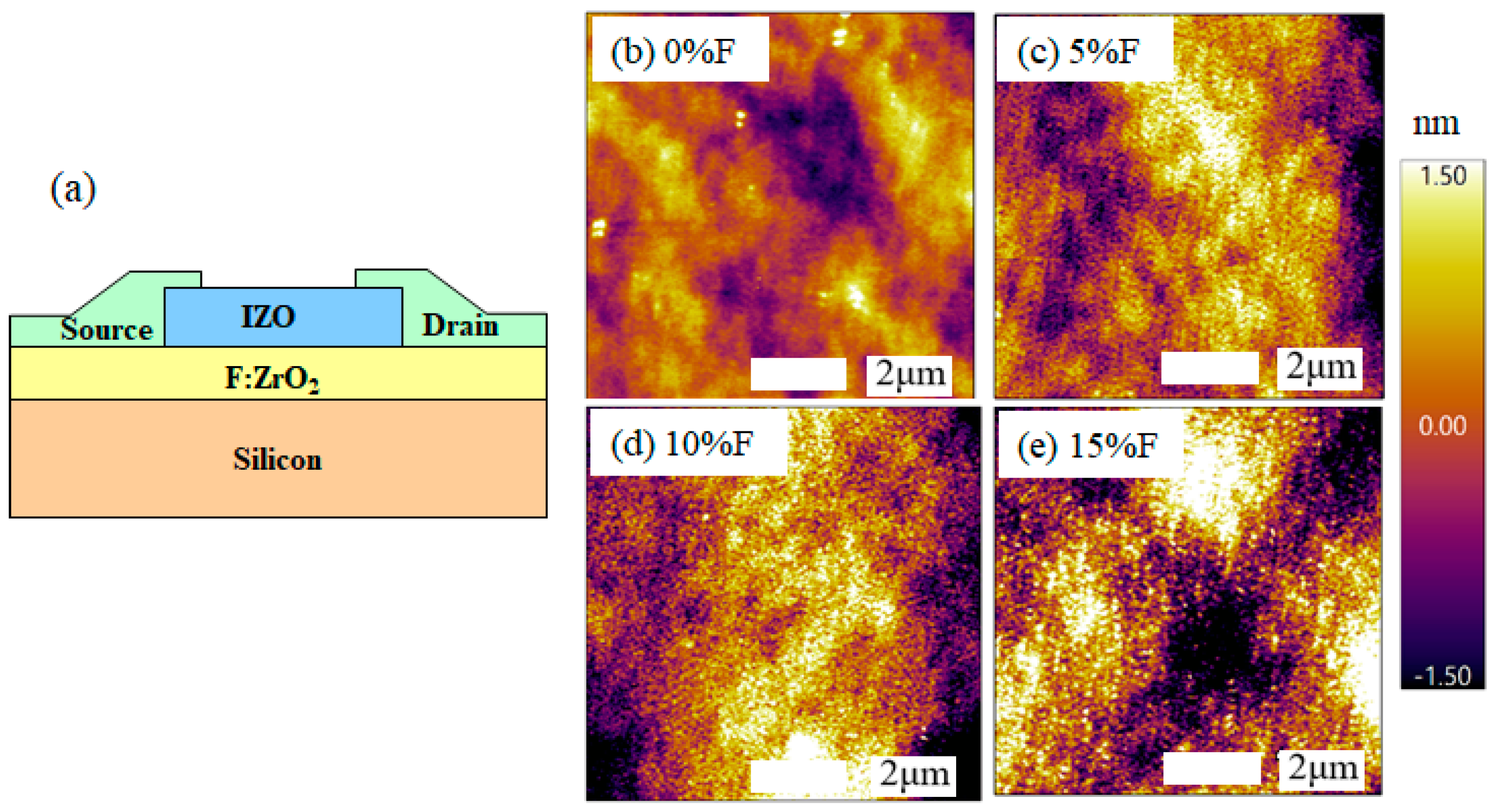
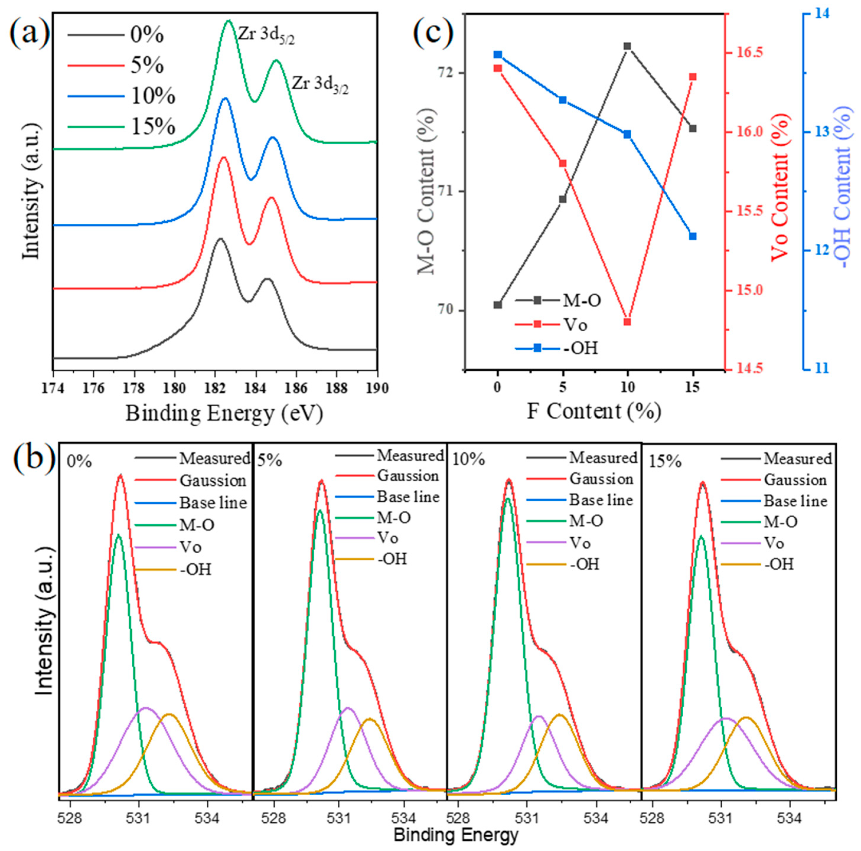
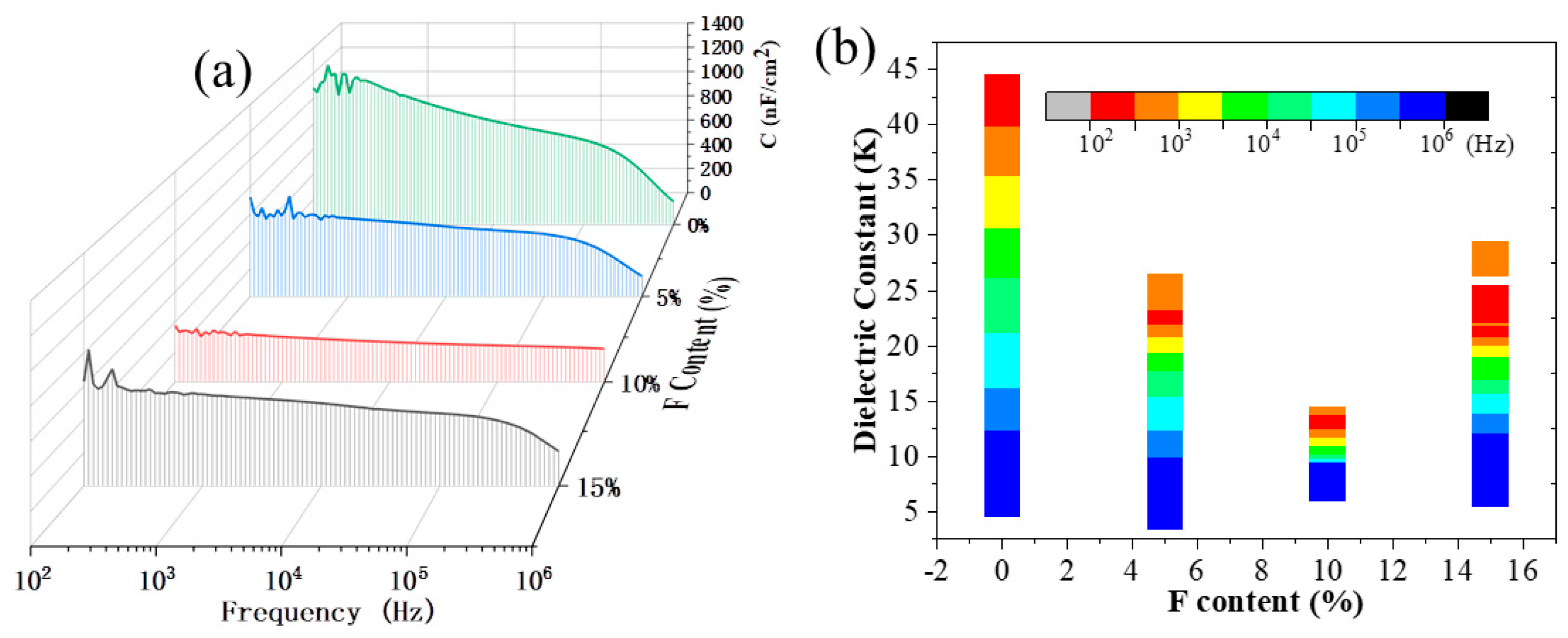
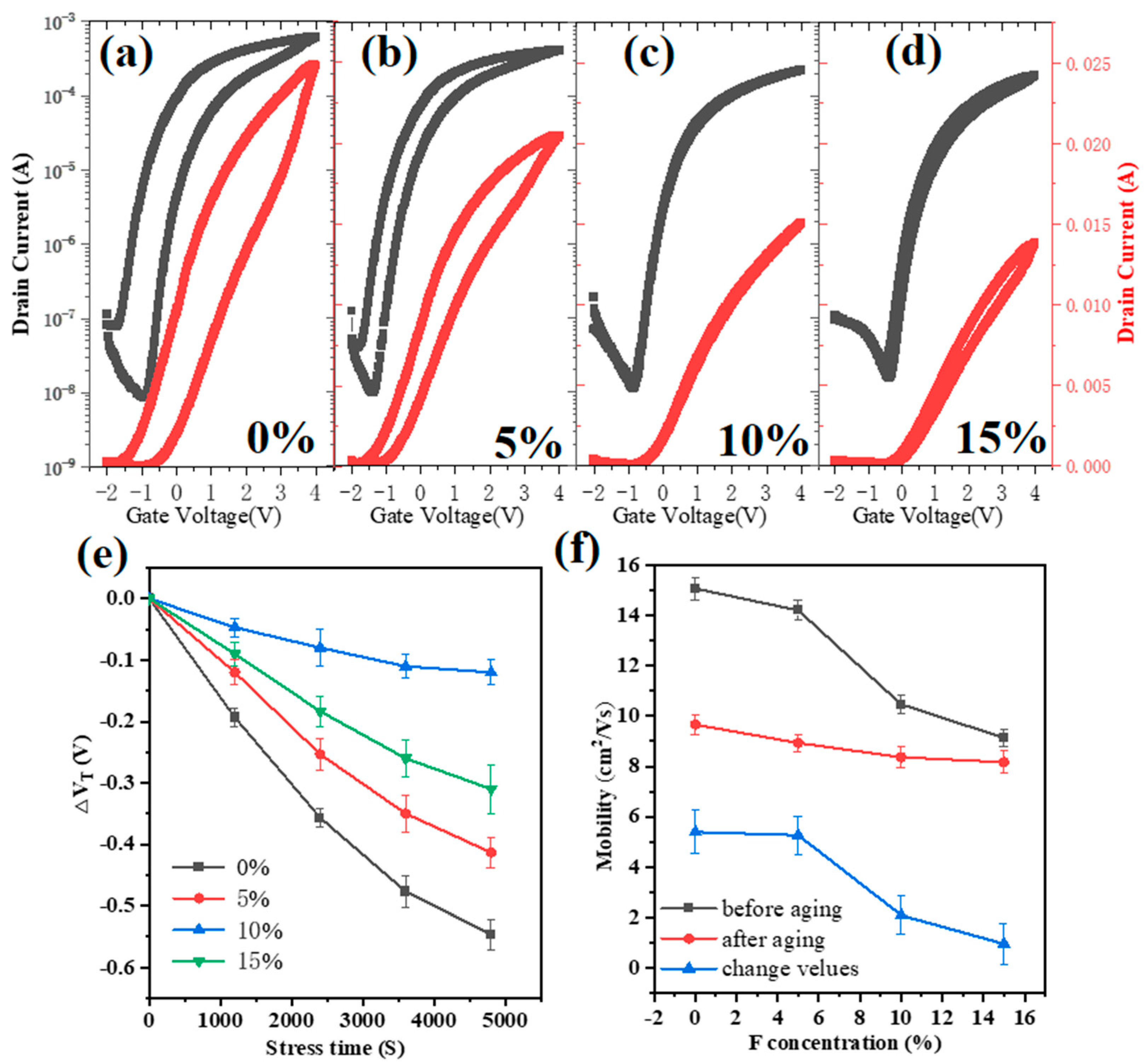
The surface morphology and roughness were characterized using a Veeco Dimension Icon atomic force microscope (AFM) in tapping mode. An X-ray photoelectron spectroscopy (XPS) analysis was conducted using an Escalab 250 Xi spectrometer (Thermo Fisher Scientific, Pardubice, Czech Republic). Film thickness was measured using a M2000U ellipsometer (J. A. Woollam, Lincoln, NE, USA) and fit with a Cauchy model. The dielectric capacitance of the MIS capacitors as a function of frequency, ranging from 20 Hz to 1 MHz, was evaluated using an Agilent E4980A precision LCR meter (Santa Rosa, CA, USA). The leakage current–voltage characteristics of the MIS capacitors and TFTs were measured using a Keithley 2450 semiconductor parameter analyzer (Cleveland, OH, USA).

3. Results

Figure 1 presents the schematic structure of the TFT, and the AFM images of ZrO2 films doped with different concentrations of fluorine. Figure 1b–e correspond to 0%, 5%, 10%, and 15% of F:ZrO2 films, respectively. These films exhibit dense and continuous surface morphologies with scattered small particles. The root mean square (RMS) roughness values are 0.473 nm, 0.488 nm, 0.539 nm, and 0.753 nm, respectively. It was observed that the surface roughness increases with the increasing doping concentration. In general, however, these F:ZrO2 films are dense, uniform, and quite smooth, making them suitable for use as insulating layers in TFTs [15,16].
Figure 2 illustrates the XPS spectra of ZrO2 films doped with varying F concentrations. In Figure 2a, the spin–orbit doublet peaks of Zr 3d (3d5/2 and 3d3/2) were observed with no additional impurity peaks. The peak centers were 182.20 and 184.60 eV, 182.40 and 184.80 eV, 182.60 and 185.00 eV, and 182.50 and 184.80 eV, respectively. The separation of 2.4 eV between the Zr 3d spin–orbit doublets suggests the presence of ionic bonding between Zr4+ and O2− in the ZrO2 films. Compared to the ZrO2 sample, the Zr 3d peak shifted 0.02 eV, 0.04 eV, and 0.03 eV towards higher binding energy for the 5%, 10%, and 15% F:ZrO2 films, respectively. This shift may be attributed to a decrease in the coordination number of metal ions in the F:ZrO2 films [17,18].
In Figure 2b, the O1s peaks of F:ZrO2 films are presented. Through Gaussian peak fitting, the O1s peak is resolved into three sub-peaks corresponding to different oxygen environments, centered at 530.02 eV, 531.37 eV, and 532.41 eV, respectively. The primary lattice peak of O1s at 530.02 eV is attributed to lattice oxygen (M-O) in metal oxides, while the peaks at 531.37 eV and 532.41 eV are associated with oxygen vacancies (VO) and hydroxyl groups (-OH) in metal hydroxides, respectively [19]. By analyzing the ratio of lattice oxygen, VO, and -OH to the total area of the O1s XPS spectrum, the relative contents could be determined, as shown in Figure 2c. This method is widely used to evaluate the quality of oxide thin films [20,21]. Through data comparison, it is evident that as the F doping concentration increases from 0% to 10%, the M-O bond ratio rises from 70.04% to 72.22%, while the Vo content decreases from 16.40% to 15.80%, and the -OH content drops from 13.65% to 12.12%. After F doping, the reduction in the Vo and -OH contents can be attributed to F occupying some of the oxygen vacancies, thereby decreasing the oxygen vacancy density [22,23]. Due to the comparable ionic radii between F⁻ and O2⁻, fluorine substitution not only mitigates structural distortions in the lattice but also replaces oxygen atoms, either generating delocalized electrons or passivating vacancy-related traps for enhanced charge transport. Additionally, the high electronegativity of F ions allows them to form hydrogen bonds with -OH, passivating the trap sites induced by -OH. However, the oxygen vacancy content of the 15% F:ZrO2 film unexpectedly increases to 16.35%, possibly due to excessive F doping leading to an increase in defects within the ZrO2 film [24].
Figure 3a illustrates the leakage–current behavior of F:ZrO2 films with varying F doping concentrations. The leakage–current density of ZrO2 was measured to be 3.5 × 10⁻⁷ A/cm2 at 2 V. This density gradually decreased to 1.8 × 10⁻⁷ A/cm2 for 5% F:ZrO2 and 8.4 × 10⁻⁸ A/cm2 for 10% F:ZrO2, likely due to F ions occupying oxygen vacancies, reducing defects, and enhancing the film’s density and insulation properties. This observation is consistent with the reduced oxygen vacancies observed in the XPS results. Conversely, the leakage current density for 15% F:ZrO2 increased to 1.2 × 10⁻⁷ A/cm2, potentially because the doped F replaced oxygen atoms, generating free electrons and increasing the carrier concentration [25]. The relationship between the leakage current density of F:ZrO2 at 2 V and the F doping concentration is depicted in Figure 2b. The highest standard deviation of the entire leakage current density was about 12.5%, which proves that the device preparation has good repeatability. Furthermore, the graph indicates that all films exhibit a high breakdown electric field, effectively preventing the insulation layer from being compromised by the gate field.
Next, capacitance–frequency curves of the Al/F:ZrO2/n++Si MIS capacitors were measured in the range of 100 Hz to 1 MHz using a bias voltage of 1 V, as illustrated in Figure 4a. The capacitance per unit area (Ci) of all F:ZrO2 films was observed to gradually decrease with increasing frequency. This phenomenon can be attributed to capacitive dispersion in the high-k material, which arises from electron polarization, ion polarization, and interfacial polarization [6,26]. The capacitance of the undoped ZrO2 film exhibited the greatest variation, ranging from 1023 nF/cm2 at 100 Hz to 206 nF/cm2 at 1 MHz. Notably, F doping consistently improved the stability of capacitance compared to the undoped ZrO2. This suggests a denser formation of M-O bonds and a lower density of defects such as oxygen vacancies (VO) and hydroxyl groups (-OH) in the thin film. On the one hand, this improvement may be due to the filling of oxygen vacancies in ZrO2 films with F ions, thereby reducing defect density. On the other hand, it could be attributed to the formation of hydrogen bonds between the doped F and hydroxyl groups, which passivate the trap sites induced by -OH, significantly reducing the number of traps in the insulating layer and, thus, minimizing capacitive dispersion [27,28]. Among the samples, the 10% F:ZrO2 film demonstrated the most stable capacitance over a broad frequency range, from 358.6 nF/cm2 at 100 Hz to 229.2 nF/cm2 at 1 MHz, which is crucial for reliable device operation at high frequencies [29,30]. However, when the F content is increased to 15%, the capacitive dispersion worsens, likely due to the introduction of additional defects caused by excessive F doping. Additionally, the thicknesses of the F:ZrO2 films, as determined by spectroscopic ellipsometry, were approximately 32.5 nm. The frequency dependence of the k values was calculated by the equation k = Cd/ε0S, where ε0 is the permittivity of a vacuum, C is the capacitance of the dielectric layer obtained from the capacitor test, S is the overlapping area of the two plates, and d is the thickness of the dielectric layer. The results are presented in Figure 4b. It is evident that the 10% F:ZrO2 film exhibits relatively stable dielectric constants.
To evaluate the suitability of F:ZrO2 films as gate dielectrics in oxide thin-film transistors, we fabricated bottom-gate IZO TFTs incorporating 0%, 5%, 10%, and 15% of F-doped ZrO2 dielectrics. Representative transfer curves of IZO/F:ZrO2 TFTs with VDS = 4 V are shown in Figure 5a–d. All samples exhibited anticlockwise hysteresis, indicating that the gate capacitance varies during continuous VGS sweeps from −2 V to 4 V and back to −2 V. Due to the higher capacitance at low frequencies under bias, the prolonged application of a larger VGS gradually increased the capacitance, leading to consistently higher capacitance during the backward sweep. Consequently, the IDS value was always greater during the backward sweep compared to the forward sweep at a given VGS, resulting in anticlockwise hysteresis [31]. For devices with an F-doped ZrO2 dielectric, improved transfer curves with reduced hysteresis were observed. Specifically, the 5% F:ZrO2-based TFT showed a reduced anticlockwise hysteresis of 0.86 V compared to the undoped ZrO2-based TFTs, which exhibited a hysteresis of 1.16 V. For 10% F:ZrO2-based TFTs, the hysteresis was only 0.12 V, suggesting that appropriate F doping significantly reduces the I-V hysteresis. This effect is likely due to F ions occupying oxygen vacancy (VO) sites in the film, thereby reducing dielectric bulk defects, enhancing film density, and minimizing the interface defects between IZO and F:ZrO2 [32]. However, for 15% F:ZrO2-based TFTs, the anticlockwise hysteresis increased to 0.26 V, possibly due to an increase in interfacial defects caused by excessive F doping. Positive gate bias stress (PBS) tests on the TFTs were conducted at VDS = 1 V for 4800 s, with the results shown in Figure 5e. The 10% F:ZrO2-based TFTs exhibited the smallest ΔVth during the gate bias process. These findings demonstrate that F doping is an effective method to enhance the bias stress stability of devices.
Given that the gate dielectric capacitance is frequency-dependent, we systematically evaluated the frequency dependence of carrier mobility. All calculations were based on the forward sweeping curve when hysteresis was observed in the devices. The results clearly indicate that undoped ZrO2-based TFTs exhibit significant mobility variations, ranging from 26.8 cm2V−1s−1 at 1 MHz to 3.5 cm2V−1s−1 at 100 Hz. Upon the fluorine doping of the gate dielectric, the mobility range significantly narrows. Notably, for 10% F:ZrO2 TFTs, the calculated mobility remained within a narrow range of 13.8 cm2V−1s−1 at 1 MHz to 7.3 cm2V−1s−1 at 100 Hz, with an average value of 10.5 cm2V−1s−1.
The electrical performance of IZO/F:ZrO2 TFTs with varying F concentrations was also assessed after three months of aging in ambient air without surface passivation. Figure 5f illustrates the fluctuations in average mobility. Specifically, the average mobility values changed as follows: from 15.1 to 9.6 cm2V−1s−1 for undoped IZO/ZrO2 TFTs, from 14.2 to 8.9 cm2V−1s−1 for 5% F:ZrO2 TFTs, from 10.5 to 8.3 cm2V−1s−1 for 10% F:ZrO2 TFTs, and from 9.1 to 8.2 cm2V−1s−1 for 15% F:ZrO2 TFTs over the three-month period. The corresponding changes in mobility gradually decreased with the increasing F concentration. These findings suggest that F ions play a crucial role in mitigating device aging [33,34].

4. Conclusions

In summary, we successfully fabricated solution-processed F:ZrO2 thin films and systematically investigated their surface morphology and oxygen defect states. It was confirmed that F ions can occupy oxygen vacancies appropriately, reducing the density of oxygen vacancies while suppressing polarization processes. The leakage–current (I–V) and capacitance–frequency (C–f) characteristics of Al/F:ZrO2/n++Si capacitors were evaluated, revealing that the F:ZrO2 dielectric exhibits low leakage current density and stable capacitance over a wide frequency range. Subsequently, metal oxide TFTs with IZO as the channel layer and F:ZrO2 as the dielectric were fabricated. The optimized 10% F:ZrO2-based TFTs exhibited reliable electrical characteristics, including high mobility across a broad frequency range from 100 Hz to 1 MHz, reduced dual-sweep hysteresis, and excellent stability under prolonged bias stress and after three months of aging. These characteristics can be attributed to the similarity in radius between F ions and O ions, which notably mitigates lattice distortion and eliminates electron traps. These results suggest that fluorine-doped ZrO2 is a promising dielectric for applications in metal oxide thin-film electronics.

Author Contributions

H.X.: Conceptualization; Data curation; Visualization; B.D.: Formal analysis; Investigation; Methodology; Resources; Software; X.Z.: Project administration; Funding acquisition; Supervision; Validation; Roles/Writing—Original draft; Writing—Review and Editing. All authors have read and agreed to the published version of the manuscript.

Funding

This work was supported by the Natural Science Foundation of Top Talent of SZTU (grant no. GDRC202304), the Natural Science Foundation of Henan Province (Grant No. 202300410036), and the National Natural Science Foundation of China (Grant No. U1504625).

Institutional Review Board Statement

Not applicable.

Informed Consent Statement

Not applicable.

Data Availability Statement

The original contributions presented in this study are included in the article. Further inquiries can be directed to the corresponding author.

Conflicts of Interest

The authors declare no conflicts of interest.

References

  1. Liang, Z.H.; Wu, W.J.; Fang, Z.Q.; Deng, Z.E.; Fu, X.; Ning, H.L.; Luo, D.X.; Zhu, Z.N.; Yao, R.H.; Peng, J.B. A review of doped metal oxide semiconductors in the stability of thin film transistors. J. Alloys Compd. 2025, 1010, 177434. [Google Scholar] [CrossRef]
  2. Kim, T.; Choi, C.H.; Hur, J.S.; Ha, D.; Kuh, B.J.; Kim, Y.; Cho, M.H.; Kim, S.; Jeong, J.K. Progress, Challenges, and Opportunities in Oxide Semiconductor Devices: A Key Building Block for Applications Ranging from Display Backplanes to 3D Integrated Semiconductor Chips. Adv. Mater. 2023, 35, 2204663. [Google Scholar] [CrossRef]
  3. Geng, D.; Wang, K.; Li, L.; Myny, K.; Nathan, A.; Jang, J.; Kuo, Y.; Liu, M. Thin-film transistors for large-area electronics. Nat. Electron. 2023, 6, 963–972. [Google Scholar] [CrossRef]
  4. Ma, L.Y.; Soin, N.; Aidit, S.N.; Rezali, F.A.M.; Hatta, S. Recent advances in flexible solution-processed thin-film transistors for wearable electronics. Mater. Sci. Semicond. Process. 2023, 165, 107658. [Google Scholar] [CrossRef]
  5. Troughton, J.; Atkinson, D. Amorphous InGaZnO and metal oxide semiconductor devices: An overview and current status. J. Mater. Chem. C 2019, 7, 12388–12414. [Google Scholar] [CrossRef]
  6. Wang, B.H.; Huang, W.; Chi, L.F.; Al-Hashimi, M.; Marks, T.J.; Facchetti, A. High-k Gate Dielectrics for Emerging Flexible and Stretchable Electronics. Chem. Rev. 2018, 118, 5690–5754. [Google Scholar] [CrossRef]
  7. Lee, H.; Islam, M.M.; Bae, J.; Jeong, M.; Roy, S.; Lim, T.; Rabbi, M.H.; Jang, J. A Coplanar Crystalline InGaO Thin Film Transistor with SiO2 Gate Insulator on ZrO2 Ferroelectric Layer: A New Ferroelectric TFT Structure. Adv. Mater. Technol. 2024, 10, 2401075. [Google Scholar] [CrossRef]
  8. Avis, C.; Jang, J. Influence of NF3 Plasma-Treated HfO2 Gate Insulator Surface on Tin Oxide Thin-Film Transistors. Materials 2023, 16, 7172. [Google Scholar] [CrossRef]
  9. Arulkumar, S.; Parthiban, S.; Eithiraj, R.D. In-Si-O thin-film transistors with atomic layer deposition-grown Al2O<sub>3</sub> gate insulator. J. Mater. Sci.-Mater. Electron. 2024, 35, 2063. [Google Scholar] [CrossRef]
  10. Cingolani, R.; Di Dio, M.; Lomascolo, M.; Rinaldi, R.; Prete, P.; Vasanelli, L.; Vanzetti, L.; Bassani, F.; Bonanni, A.; Sorba, L.; et al. Photocurrent spectroscopy of Zn1−xCdxSe/ZnSe quantum wells in p-i-n heterostructures. Phys. Rev. B 1994, 50, 12179–12182. [Google Scholar] [CrossRef]
  11. Kosacki, I.; Suzuki, T.; Petrovsky, V.; Anderson, H.U. Electrical conductivity of nanocrystalline ceria and zirconia thin films. Solid State Ion. 2000, 136, 1225–1233. [Google Scholar] [CrossRef]
  12. Lee, S.; Nam, J.; Choi, Y.; Jeong, J.; Nam, M.K.; Oh, H.; Kim, H.; Park, Y.; Kim, Y.; Jeon, W. Achieving Equivalent Oxide Thickness Scaling of a ZrO2 Dielectric Thin Film via Gd Doping without Sacrificing Tetragonal Crystallinity. Acs Appl. Electron. Mater. 2024, 6, 8979–8986. [Google Scholar] [CrossRef]
  13. Zhuang, X.M.; Patel, S.; Zhang, C.; Wang, B.H.; Chen, Y.; Liu, H.Y.; Dravid, V.P.; Yu, J.S.; Hu, Y.Y.; Huang, W.; et al. Frequency-Agile Low-Temperature Solution-Processed Alumina Dielectrics for Inorganic and Organic Electronics Enhanced by Fluoride Doping. J. Am. Chem. Soc. 2020, 142, 12440–12452. [Google Scholar] [CrossRef]
  14. Wolf, D.; Lubk, A.; Prete, P.; Lovergine, N.; Lichte, H. 3D mapping of nanoscale electric potentials in semiconductor structures using electron-holographic tomography. J. Phys. D Appl. Phys. 2016, 49, 364004. [Google Scholar] [CrossRef]
  15. Tsai, J.T.H.; Lee, B.H.B.; Yang, M.S. Fabrication of ZnO thin film transistors by atomic force microscopy nanolithogrophy through zinc thin films. Phys. Rev. B 2009, 80, 245215. [Google Scholar] [CrossRef]
  16. Chang, P.C.; Lee, J.; Huang, D.; Subramanian, V.; Murphy, A.R.; Frechet, J.M.J. Film morphology and thin film transistor performance of solution-processed oligothiophenes. Chem. Mater. 2004, 16, 4783–4789. [Google Scholar] [CrossRef]
  17. Kumar, A.; Mondal, S.; Rao, K. Low temperature solution processed high-κ ZrO2 gate dielectrics for nanoelectonics. Appl. Surf. Sci. 2016, 370, 373–379. [Google Scholar] [CrossRef]
  18. Panda, D.; Tseng, T.Y. Growth, dielectric properties, and memory device applications of ZrO2 thin films. THIN SOLID Film. 2013, 531, 1–20. [Google Scholar] [CrossRef]
  19. Mativenga, M.; Haque, F.; Billah, M.M.; Um, J.G. Origin of light instability in amorphous IGZO thin-film transistors and its suppression. Sci. Rep. 2021, 11, 14618. [Google Scholar] [CrossRef]
  20. Kim, H.; Maeng, S.; Lee, S.; Kim, J. Improved Performance and Operational Stability of Solution-Processed InGaSnO (IGTO) Thin Film Transistors by the Formation of Sn-O Complexes. Acs Appl. Electron. Mater. 2021, 3, 1199–1210. [Google Scholar] [CrossRef]
  21. Li, J.; Zhou, Y.-H.; Zhong, D.-Y.; Zhang, J.-H. Fluorine-controlled subgap states and negative bias illumination stability behavior in solution-processed InZnOF thin-film transistor. Appl. Phys. A 2019, 125, 527. [Google Scholar] [CrossRef]
  22. Lin, Z.Y.; Kang, L.; Zhao, J.X.; Yin, Y.; Wang, Z.H.; Yu, J.; Li, Y.; Yi, G.Z.; Nathan, A.; Li, X.Y.; et al. The Role of Oxygen Vacancy and Hydrogen on the PBTI Reliability of ALD IGZO Transistors and Process Optimization. IEEE Trans. Electron Devices 2024, 71, 3002–3008. [Google Scholar] [CrossRef]
  23. Kim, H.G.; Lee, H.J.; Lee, K.M.; Kim, T.G. Improved mobility and bias stability of Hf-doped IGZO/IZO/Hf-doped IGZO thin-film transistor. J. Alloys Compd. 2024, 981, 173587. [Google Scholar] [CrossRef]
  24. Xie, Z.J.; Li, X.H.; Liu, H.X.; Tang, J.; Wang, H. Improvement of Threshold Voltage With ZrO2/HfO2 Gate Dielectric and CF4 Plasma Treatment on AlGaN/GaN HEMT. IEEE Electron Device Lett. 2024, 45, 1125–1128. [Google Scholar] [CrossRef]
  25. Lee, J.S.; Chang, S.; Koo, S.M.; Lee, S.Y. High-Performance a-IGZO TFT With ZrO2 Gate Dielectric Fabricated at Room Temperature. IEEE Electron Device Lett. 2010, 31, 225–227. [Google Scholar] [CrossRef]
  26. Jiang, G.X.; Liu, A.; Liu, G.X.; Zhu, C.D.; Meng, Y.; Shin, B.; Fortunato, E.; Martins, R.; Shan, F.K. Solution-processed high-k magnesium oxide dielectrics for low-voltage oxide thin-film transistors. Appl. Phys. Lett. 2016, 109, 183508. [Google Scholar] [CrossRef]
  27. Seo, J.S.; Jeon, J.H.; Hwang, Y.H.; Park, H.; Ryu, M.; Park, S.H.K.; Bae, B.S. Solution-Processed Flexible Fluorine-doped Indium Zinc Oxide Thin-Film Transistors Fabricated on Plastic Film at Low Temperature. Sci. Rep. 2013, 3, srep02085. [Google Scholar] [CrossRef] [PubMed]
  28. Sil, A.; Goldfine, E.A.; Huang, W.; Bedzyk, M.J.; Medvedeva, J.E.; Facchetti, A.; Marks, T.J. Role of Fluoride Doping in Low-Temperature Combustion-Synthesized ZrOx Dielectric Films. ACS Appl. Mater. Interfaces 2022, 14, 12340–12349. [Google Scholar] [CrossRef]
  29. Liu, A.; Zhu, H.H.; Guo, Z.D.; Meng, Y.; Liu, G.X.; Fortunato, E.; Martins, R.; Shan, F.K. Solution Combustion Synthesis: Low-Temperature Processing for p-Type Cu:NiO Thin Films for Transparent Electronics. Adv. Mater. 2017, 29, 1701599. [Google Scholar] [CrossRef]
  30. Xu, W.Y.; Wang, H.; Ye, L.; Xu, J.B. The role of solution-processed high-κ gate dielectrics in electrical performance of oxide thin-film transistors. J. Mater. Chem. C 2014, 2, 5389–5396. [Google Scholar] [CrossRef]
  31. Li, Y.X.; Liang, R.R.; Wang, J.B.; Jiang, C.S.; Xiong, B.K.; Liu, H.F.; Wang, Z.B.; Wang, X.F.; Pang, Y.; Tian, H.; et al. Negative Capacitance Oxide Thin-Film Transistor With Sub-60 mV/Decade Subthreshold Swing. IEEE Electron Device Lett. 2019, 40, 826–829. [Google Scholar] [CrossRef]
  32. Dutta, G.; Hembrarn, K.; Rao, G.M.; Waghmare, U.V. Enhanced dielectric response of ZrO2 upon Ti doping and introduction of O vacancies. J. Appl. Phys. 2008, 103, 016102. [Google Scholar] [CrossRef]
  33. Lim, W.; Kim, S.H.; Wang, Y.L.; Lee, J.W.; Norton, D.P.; Pearton, S.J.; Ren, F.; Kravchenko, I.I. Stable room temperature deposited amorphous InGaZnO4 thin film transistors. J. Vac. Sci. Technol. B 2008, 26, 959–962. [Google Scholar] [CrossRef]
  34. Boratto, M.H.; Scalvi, L.V.A.; Goncharova, L.V.; Fanchini, G. Effects of Solution History on Sol-Gel Processed Tin-Oxide Thin-Film Transistors. J. Am. Ceram. Soc. 2016, 99, 4000–4006. [Google Scholar] [CrossRef]
Figure 1. (a) Schematic structure of the TFT. Atomic force microscopy (AFM) images of F:ZrO2 thin films with varying fluorine doping concentrations: (b) 0%, (c) 5%, (d) 10%, and (e) 15%.
Materials 18 01980 g001
Figure 2. XPS spectra of F:ZrO2 thin films with different F doping concentrations. (a) Zr 3d spectra; (b) best-fit results for O1s peaks. (c) Atomic percentages of M-O, VO, and -OH bonds as a function of the F content.
Materials 18 01980 g002
Figure 3. (a) The leakage current–voltage characteristic curves of F:ZrO2 films with different F concentrations. (b) The leakage current density as a function of F concentrations.
Materials 18 01980 g003
Figure 4. (a) Capacitance–frequency plots in the range of 100 Hz to 1 MHz for F:ZrO2 films with different F concentrations. (b) The corresponding dielectric constants are shown at the indicated frequencies.
Materials 18 01980 g004
Figure 5. (ad) Transfer curves of IZO/F:ZrO2 TFTs with different F concentrations. (e) The threshold voltage shift of ΔVth after a 4800 s gate bias was applied. (f) The fluctuations in average mobility of these devices after three months.
Materials 18 01980 g005
Disclaimer/Publisher’s Note: The statements, opinions and data contained in all publications are solely those of the individual author(s) and contributor(s) and not of MDPI and/or the editor(s). MDPI and/or the editor(s) disclaim responsibility for any injury to people or property resulting from any ideas, methods, instructions or products referred to in the content.

