Article

Voltage-Controlled Spin-Orbit-Torque-Based Nonvolatile Flip-Flop Designs for Ultra-Low-Power Applications

1
School of Electronic and Information Engineering, Beihang University, Beijing 100191, China
2
College of Electronic Information and Engineering, Nanjing University of Aeronautics and Astronautics, Nanjing 210016, China
3
School of Integrated Circuit Science and Engineering, Fert Beijing Institute, Beihang University, Beijing 100191, China
*
Author to whom correspondence should be addressed.
Appl. Sci. 2023, 13(20), 11316; https://doi.org/10.3390/app132011316
Submission received: 14 September 2023 / Revised: 6 October 2023 / Accepted: 13 October 2023 / Published: 15 October 2023
(This article belongs to the Special Issue Advanced Integrated Circuits and Devices)

Abstract

:
Flip-flop (FF) serves as a fundamental unit in various sequential logic circuits and complex digital electronic systems for generating, transforming, and temporarily storing digital signals. Nonvolatility plays a crucial role in FFs by ensuring instant data recovery after unexpected data loss. Nonvolatile flip-flop can quickly recover in a self-powered environment, making it suitable for application environments such as the Internet of Things (IOT). Unfortunately, most existing nonvolatile FFs (NVFFs) suffer from extended delays and high energy consumption during data backup and restore operations. In this paper, we propose two innovative voltage-controlled nonvolatile FFs (VC-FFs), namely VC-DFF (voltage-controlled D-FF) and VC-SRFF (voltage-controlled SR-FF), which address these challenges using voltage-controlled spin-orbit torque (VC-SOT) devices. The proposed designs are evaluated using a 40 nm CMOS process. Simulation results demonstrate that the proposed designs achieve significant improvements in write (recovery) energy consumption, with over 7.2× (1.54×) and 18.7× (2×) enhancements compared to their STT- and SOT-based counterparts, respectively.

1. Introduction

With the continuous development of the Internet of Things, various IoT devices have been integrated into our daily lives. Due to the complexity of the working environment and the requirement for portability of portable devices, these IoT devices do not meet the conditions to be equipped with high-capacity batteries or wired power supplies [1]. The energy supply in the Internet of Things environment is mostly obtained through changes in external environments such as solar energy, wind energy, and vibration. This constantly changing and unpredictable external environmental change may lead to an unstable energy supply [2], leading to frequent power outages and system restarts. Flip-flop (FF) is a basic unit in sequential logic circuits that can be used to store and transfer temporary digital signals. The traditional FFs are composed of CMOS devices, which can realize basic operations such as resetting, setting, triggering, and maintenance. SR flip-flop (SRFF) and D flip-flop (DFF) are two typical representatives of basic FFs, which can be used as the basis for designing other types of FFs. As shown in Figure 1, for CP = “0”, the output Q and QB of the SRFF (or DFF) only depend on the initial states. For CP = “1”, the state tradition diagrams of the SRFF and DFF are shown in Figure 1b,d, respectively. FF is a typical volatile device, which means that power outages can cause data loss.
The inability to predict the time and location of the next outage from an unstable power supply makes data protection a key challenge. If the FF is nonvolatile and is able to maintain the state after powering off, the whole system can support transient data recovery. Recently, nonvolatile FF (NVFF) has attracted great interest in power-gating applications and a number of NVFF designs have been proposed by integrating nonvolatile memory (NVM) devices [1,2,3,4,5,6,7]. In the NVFFs, data are first stored in the NVMs when the system is in the standby state, and they are then restored back into the regular FFs when the system is powered on [8,9,10,11,12,13,14,15,16]. In this case, run-time data can be maintained even if a power interruption happens.
Nevertheless, most of the current nonvolatile FFs (NVFFs) suffer from long delays and high energy in the data backup and restore operations. Many efforts have been made and many NVFF designs have been proposed to minimize the latency needed for data transportation. Biglari et al. presented two bipolar ReRAM-based NVFFs [17]. In this design, both the endurance and the energy efficiency are improved. In addition, an area-efficient NVFF based on a spin-torque transfer magnetic tunnel junction (STT-MTJ) was proposed [18]. It has an improvement of nearly a factor of 4–23 in terms of area overhead compared to previous NVFF architectures. To reduce the energy, Deng et al. proposed four NVFF designs based on either DFF or SRFF architecture and perpendicular MTJs (pMTJs) [19]. These designs can achieve a fast reading speed (<200 ps), low read power (<10 fJ), and high area efficiency. However, when the power supply is unstable or the system is frequently powered off, the above designs cannot work normally. Some NVFFs [10,11,15,20] involve a power supply state detection circuit, so that data can be backed up into NVMs in time when the system is powered off. Nevertheless, these additional circuits not only increase the complexity but also degrade the performance. To achieve shorter delay and better area efficiency, Chang et al. proposed a memristor-based NV-DFF [21]. In ref. [21], the functions are accomplished by reading and writing RRAM devices. However, the repeated reading and writing operations of RRAM devices bring high delay and high power consumption. On the other hand, NVFFs using magnetic tunnel junctions (MTJs) are the most popular candidates. MTJ has the advantages of nonvolatility, low power consumption and high speed. It can be programmed using different methods, such as field-induced magnetization (FIM) reversal, spin transfer torque (STT), and spin-orbit torque (SOT). FIM requires an external magnetic field to program the MTJ, which increases energy consumption and hinders its scalability. STT needs a large drive current, which brings high write power consumption, and the same read–write operation path will also bring read–write crosstalk problems. Recently, a new MTJ device with an in-plane exchange bias (EB) called voltage-controlled spin-orbit torque (VC-SOT) has received extensive attention from academia and industry [22]. With the aid of an in-plane exchange bias, the VC-SOT MTJ can be switched without an additional field. By controlling the bias voltage applied to the MTJ and the bidirectional SOT current through the anti-ferromagnetic (AFM) layer, the MTJ can be switched at a fast speed. In addition, the read–write current of the VC-SOT MTJ device is lower than that of STT-MTJ and SOT-MTJ devices. The lower current makes the VC-SOT MTJ device consume less energy during the read and write operations.
In this paper, based on the VC-SOT-MTJ device, we propose two novel NVFFs, making the following main contributions:
(1)
We proposed a symmetric complementary scheme, employing two back-to-back connected VC-SOT-MTJ devices to enable fast data configuration and a high reading threshold;
(2)
We proposed a simple working method for the NVFF to enable traditional FF functions and nonvolatility;
(3)
We proposed two high-speed, energy-efficient VC-FF designs with simpler circuit structures and lower area overhead.
The remainder of this paper is organized as follows: Section 2 introduces the basic structure and operation of the VC-SOT MTJ device; Section 3 illustrates the operation mechanism of the proposed VC-DFF and VC-SRFF; Section 4 presents the experimental results; finally, Section 5 concludes the paper.

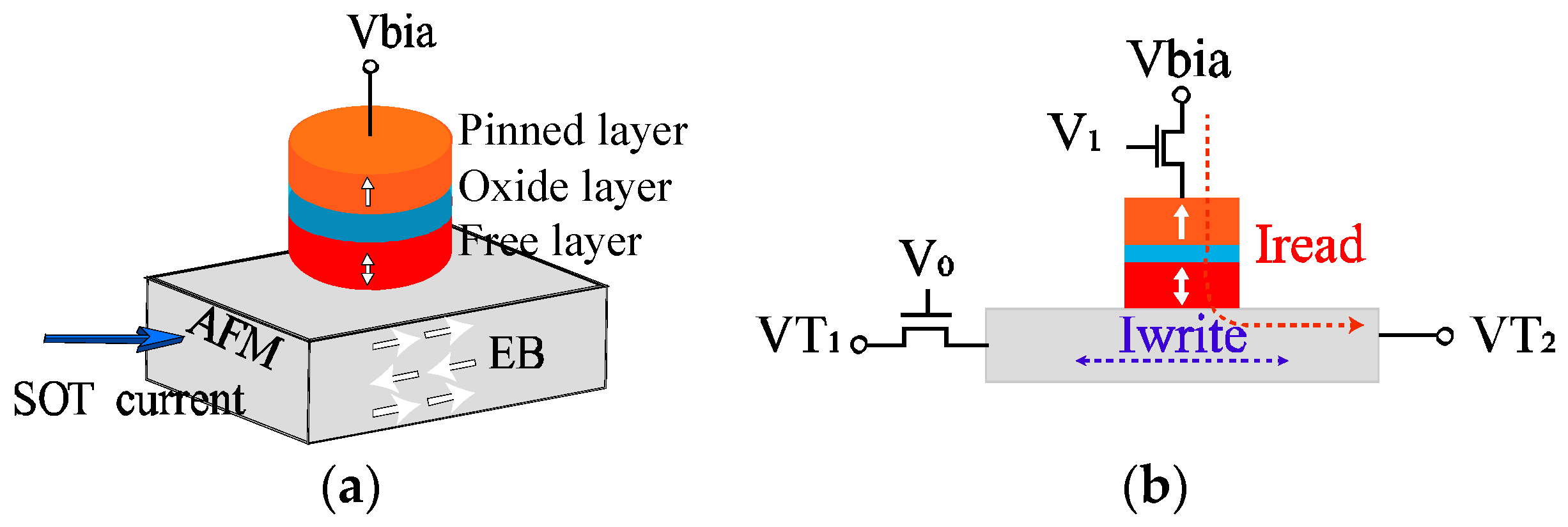
2. Basic Structure of the VC-SOT MTJ Device

Spintronic devices achieve the injection, transport, and detection of spin current by regulating the spin properties of electrons, thereby achieving the processing, transmission, and representation of electronic signals. Magnetic tunnel junction is a way to control electron spin in spintronics. By adjusting the magnetization direction of the ferromagnetic layer in the magnetic tunnel junction, it exhibits different macroscopic electrical characteristics, such as resistance, performed to achieve data storage or calculation. The methods of regulating magnetic tunnel junctions generally include applying magnetic fields, currents, and voltages.
A typical VC-SOT MTJ structure (Figure 2a) contains an anti-ferromagnetic (AFM) layer (e.g., IrMn) with an MTJ positioned on top of it. The MTJ consists of three layers: the ferromagnetic (FM, e.g., CoFeB) pinned layer, the oxide layer (e.g., MgO), and the FM-free layer. The magnetization direction of the pinned layer remains fixed, while the free layer’s magnetization direction can be freely altered. When the magnetization direction of the free layer is anti-parallel (AP) to the pinned layer, the MTJ is in a high resistance state. Conversely, when the magnetization direction of the free layer is parallel (P) to the pinned layer, the MTJ is in a low resistance state. These two resistive states of the MTJ can represent data “1” and “0” (AP for “1”, P for “0”). A recent discovery involves a novel magnetic field-free switching mechanism [19], which utilizes an IrMn/CoFeB/MgO structure and achieves field-free SOT switching aided by an in-plane EB. As shown in Figure 2a, the new mechanism also incorporates the voltage control of the magnetic anisotropy (VCMA) effect, significantly reducing the SOT switching current by applying a bias gate voltage (Vbia). The magnetization of the free layer in the MTJ device can be pulled towards the in-plane direction by both the SOT and voltage torques. In addition, in-plane magnetic symmetry is disrupted by the exchange bias between the AFM/FM (IrMn/CoFeB) layers of the MTJ. In sub-nanoseconds, the deterministic and complete reversal of the magnetization in the free layer of the MTJ device can be achieved.
Figure 2b shows a typical VC-SOT MTJ bit-cell structure. It consists of a VC-SOT MTJ and two NMOS transistors. During the write operation, for V0 = “1”, a write voltage is applied between VT1 and VT2 to generate a write current (Iwrite). The magnetization direction of the free layer of MTJ is then switched based on the direction of Iwrite. Simultaneously, V1 = “1”, and a bias voltage (Vbia) is connected to the MTJ, reducing the energy barrier required for the magnetization direction switch. The read operation follows a different path. Specifically, during the read operation, the read current (Iread) flows through the MTJ, with the MTJ state determining the amplitude of Iread.

3. Proposed VC-FFs

Traditional NVFFs generally include a power state detection circuit, control circuit, volatile FF circuit, nonvolatile memory and peripheral read–write circuits. When the NVFF encounters an unexpected power failure, the power supply state detection circuit can detect the power supply state and transmit the signal to the control circuit. The control circuit controls the read–write circuits of the NVFF for data backup operation. Compared with the traditional NVFFs, the VC-FFs proposed in this paper consist of basic CMOS transistors and VC-SOT-MTJ devices. The proposed VC-FFs can realize the basic functions of traditional FFs with nonvolatility. The circuit structure and working principle are much simpler compared to previous NVFF designs. This section presents the schematic and principle of the VC-DFF and VC-SRFF.

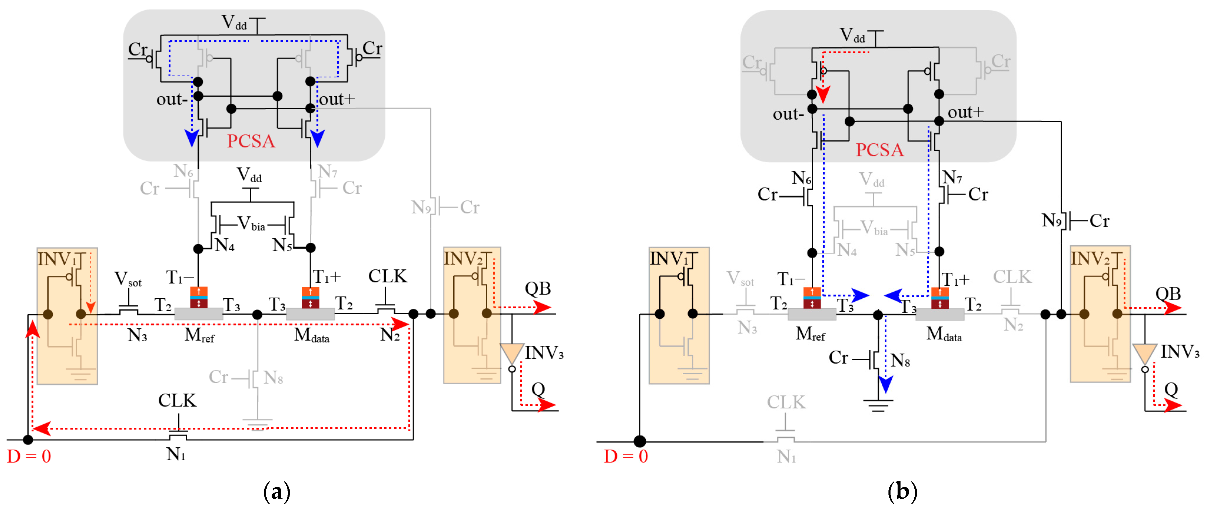
3.1. VC-DFF Circuit Architecture and Operations
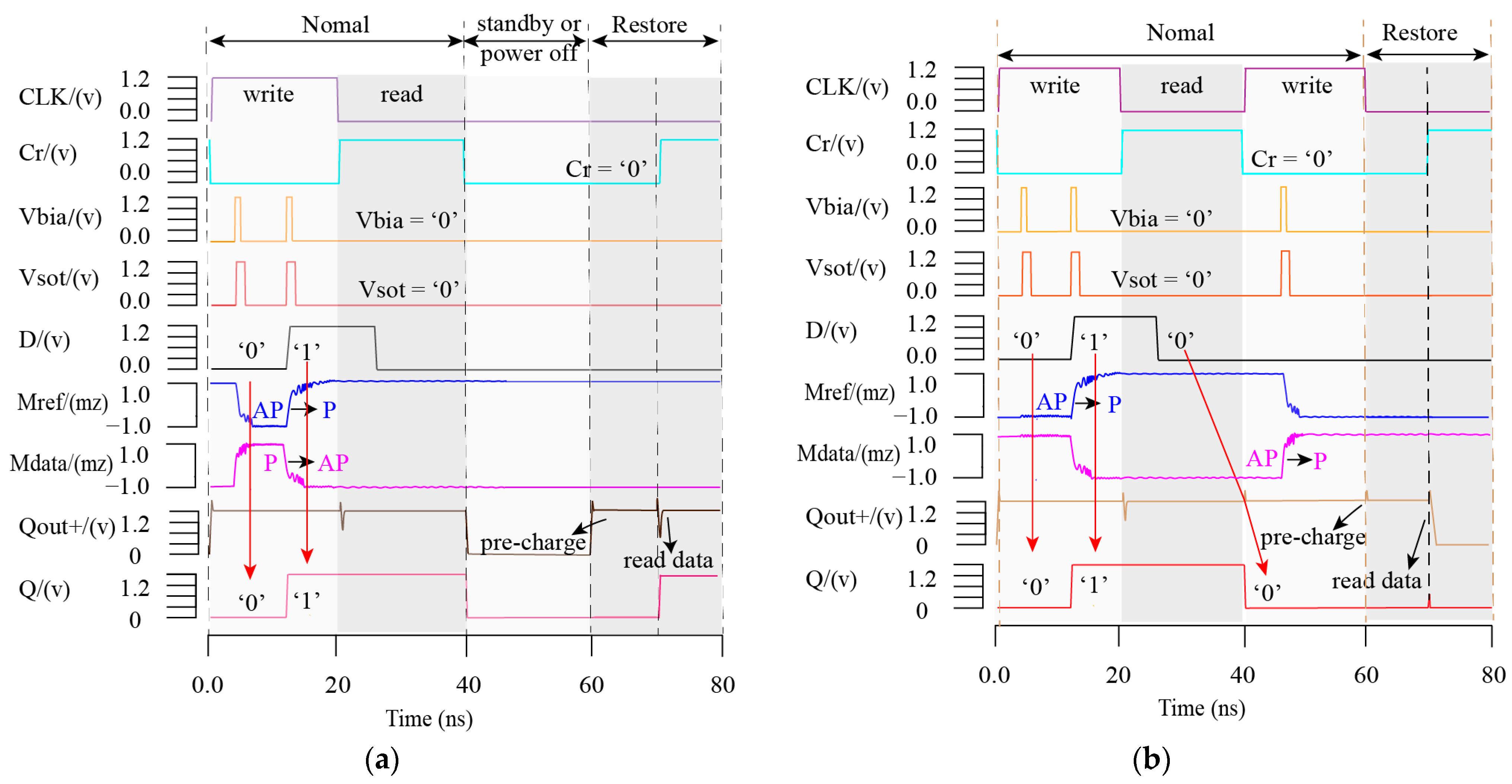
The architecture of the VC-DFF is illustrated in Figure 3. It mainly consists of two VC-SOT MTJs (Mdata and Mref), four control transistors (N2~N5), five transmission transistors (N1 and N6~N9), three inverters (INV1~INV3) and a pre-charge sensing amplifier (PCSA) [20,23]. In this architecture, D represents the input data. CLK and CLKB are two complementary clock signals. Q and QB represent two complementary output signals. Mdata and Mref are data cell and reference cells, respectively, used to store one single bit. Cr represents the read control signal, which is employed to read the data stored in the MTJ device. It is defined by the following formula:
C r = 0 ,             0 t < T 4 1 ,             T 4 t < T 2 CLKB ,                 t T 2 a = 1 ,
where T represents a clock cycle. The control signal Cr is always consistent with CLKB, except for the first half of the clock cycle. The VC-DFF uses a symmetric complementary scheme, where two MTJs are used to store one bit. As shown in Figure 3, both the T3 terminals of Mdata and Mref are shorted to ensure the opposite direction of the writing current. It is noted that Mdata and Mref are in complementary states. This complementary approach for data storage improves the read margin of the PCSA. The increase in the read margin greatly improves the speed and reliability. The working status of the VC-DFF can be divided into normal mode, standby/power off mode, and recovery mode, based on the power supply status of the circuit.

3.1.1. Normal Mode

In this state, the traditional NVFF [14,15,16,17,18] separates the MTJs from the FF circuits via the transmitting transistors. As a result, the NVFFs work like traditional FFs. However, if the data are not backed up in time, there is still a risk of data loss, especially in the case of intermittent powering off. Traditional NVFFs need to perform the data backup operation before switching off the power supply in case of unexpected power failure. Unlike the traditional NVFFs, the proposed VC-DFF does not easily lose the data of the DFF. The input data can be saved in normal operation mode, so the VC-DFF does not require an additional backup operation in case of system power failure. In this state, the signal Cr is determined by the signal CLKB. As shown in Figure 3a, when CLK = “1”, N1 turns on while N6~N9 turn off. The state of Q is consistent with that of the input signal D. The state diagram of the VC-DFF is the same as shown in Figure 1d. The voltages of the two write control signals Vsot and Vbia are set to Vdd. N4 and N5 are turned on, and the bias voltages of MTJs (Mdata and Mref) rise to Vdd. Increasing the bias voltage reduces the energy barrier of the VC-MTJ devices. It is particularly noteworthy that the two VC-SOT-MTJ devices are connected back to back. The structure can ensure that the magnetization direction of two devices is always reversed to a complementary state when the write current passes through the two devices. Specifically, for D = “0”, a SOT write current flows from Mref to Mdata. The write operation is completed by switching the magnetization of Mref and Mdata to the AP (“1”) and P (“0”) states, respectively. It should be noted that the voltage of Cr is always locked at GND when CLK = “1”, causing the node out+ (out) in the PCSA to rise to V d d before the read operation. As shown in Figure 2b, when CLK = “0”, N6~N9 turn on while N1~N5 turn off. In this case, Q follows the state of out+. The data voltage signal (VT1+) and the reference voltage signal (VT1−) are involved in the sensing operation of the PCSA. Finally, the PCSA generates the readout output. As mentioned above, data are always stored in a complementary state in the MTJ devices. Therefore, this symmetrical structure can maximize the read margin and the stability of the PCSA.

3.1.2. Standby/Power off Mode

When the system is unexpectedly powered down, the traditional NVFFs require an additional power supply state detection circuit to determine when the data are backed up or restored. The detection circuit makes the circuit more complicated, and the detection and backup/reduction operations also increase the energy consumption and latency. Note that the VC-DFF completes the storage of data in the VC-SOT MTJs during normal working mode. The controller can power off unused modules to reduce the static power consumption. Even if a power interruption occurs, there is no need for additional state detection and data backup operations to handle the power interruption.

3.1.3. Restore Mode

After the power supply is restored, only the read operation of the MTJs is required. According to Equation (1), with an appropriate excitation signal Cr, data stored in MTJs can be read out by the PCSA for data recovery. As can be seen, the input data D are stored in the nonvolatile MTJ during the normal mode. After the power supply is restored, only the read operation of the MTJs is required. The VC-DFF can realize ultra-low energy consumption during the recovery operation, without any stationary currents and dynamic charging/discharging currents. Due to the absence of backup operations, the VC-DFF avoids the power, delay and area overhead for data backup. Compared to existing designs, our work achieves higher speed and energy efficiency.

3.2. VC-SRFF Circuit Architecture and Operations

Figure 4 illustrates the VC-SRFF structure, which shares a similar working principle to the VC-DFF proposed in Section 3.1. To explain the VC-SRFF’s working principle, we use the example of setting R = “0”, S = “1”. As shown in Figure 4a, when CLK = “1”, N1 is turned on while N6~N9 are turned off. Consequently, an SOT writes current flows from Mref to Mdata, writing the data “1” and “0” into Mref and Mdata, respectively. Simultaneously, the PCSA performs the pre-charging operation. When CLK = “0”, N6~N9 are turned on while N1~N5 are turned off. In this scenario, Q follows the state of out+. The sensing operation of the PCSA involves the data voltage signal (VT1+) and the reference voltage signal (VT1−). Finally, the PCSA generates the readout output. The standby/power off mode and restore mode are not different from VC-DFF.

4. Simulations and Discussions

Based on the circuits shown in Figure 3 and Figure 4, the proposed VC-DFF and VC-SRFF are designed and evaluated using a 40 nm CMOS design kit. The parameters of the VC-SOT MTJ and variables are summarized in Table 1.
Figure 5 presents the transient simulation waveforms of the VC-DFF. As shown in Figure 5a,b, the VC-DFF begins with a normal mode (writing process and reading process), which is consistent with the description in Section 3.1.1. During the writing process, since Cr is always set to “0” and the PCSA circuit remains in the pre-charging stage, resulting in OUT+ = OUT = “1”. The output value Q changes accordingly with D. When performing a write operation, Vbia and Vsot need to apply a positive pulse voltage (pulse width of 1 ns and 1.2 ns, respectively). As shown in Figure 5a, when D = ‘0’ and Vsot and Vbia apply a positive pulse voltage, the magnetization direction of the MTJ device in Mdata transitions from the AP to P state, completing nonvolatile storage of data “0”. When D changes from “0” to “1”, the magnetization direction of the MTJ device in Mdata changes from P to AP state, completing the nonvolatile storage of data “1”. The main difference between Figure 5a and b lies in the difference in the initial data stored in Mdata. From Figure 5b, it can be seen that when the written data are consistent with the original data, the magnetization direction of MTJ does not change. The simulation results show that the write delay of the MTJ device is 4 ns. The states of Mdata and Mref are always complementary.
During the read process, CLK is set to “0” and Cr is set to “1”. The output Q during the reading process depends on the latest written data (“1”) from the previous writing process. During the reading process, when D changes, the output result remains unchanged. The VC-DFF does not require any additional operations when the system cuts off the module power to save energy or encounters an unexpected power off, as shown in Figure 5a.
The recovery mode essentially performs a reading operation of the resistance state stored in Mdata by the PCSA circuit. As shown in Figure 5a, when the state of Mdata is AP, the output value Q during the recovery process is “1”. As shown in Figure 5b, when the state of Mdata is P, the output value Q during the recovery process is “0”, which is consistent with the expected result. The simulation results in Figure 5 demonstrate that the VC-DFF can successfully operate in the modes, achieving data recovery and normal reading and writing processes.
Figure 6 presents the transient simulation waveforms of the VC-SRFF. In the normal mode, the VC-SRFF functions similarly to the VC-DFF. When S and R are set to different logic levels, and the output terminals Q and QB have two complementary stable states. As shown in Figure 6, when S = “0” and R = “1”, a SOT write current flows from Mref to Mdata. The write operation is achieved by switching the magnetization of Mref and Mdata to AP and P, respectively. When S = “1” and R = “0”, a SOT write current flows from Mref to Mdata. The magnetizations of Mref and Mdata are switched to P and AP states, respectively. During the read processes, the output result Q is not affected by changes in S and R. The value of Q is the data stored in Mdata after the last write operation. The operation in the data recovery phase is the same as the operation process in VC-DFF, which essentially involves reading the data stored in MTJs. The simulation results in Figure 6 show that VC-SRFF works successfully in all modes.
Table 2 compares the performance of our work with the state-of-the-art NVFFs [8,12,19,24]. As can be seen, ref. [8] has a certain area advantage, but it has a large read–write power consumption. However, the total number of devices in this paper represents the number of all devices involved in the work, while the number of devices in the STT-based NVFF [12,24] and the SOT-based NVFF [8,19] does not include the number of devices in the peripheral state detection circuit. Compared to the STT-based NVFF [12,24], our work can achieve up to a 20× (1.4×) reduction in write latency. Moreover, in terms of write power consumption, our work shows up to a 718× (7.2×) and 18.7× (31×) improvement compared to the STT-based NVFF [12,24] and the SOT-based NVFF [8,19], respectively. Additionally, the recovery power consumption of the STT-based NVFF [8,12] is 1.54 (3.47) times that of our work, while the SOT-based NVFF is about twice that of our work. The main reason for the significant reduction in write and recovery power consumption is the complexity of the circuit architecture. Specifically, the STT-based NVFF not only requires an additional system power state detection circuit for backup and restore operations but also additional write circuits and complex control logic gates for data-writing operations. In comparison, the SOT-based NVFF only requires a system power state detection circuit, resulting in a simpler circuit design. The VC-FFs we propose do not require additional peripheral circuits. Therefore, among these three designs, our work exhibits the simplest structure and best performance. Although VC-FFs provide very low read and write power consumption for nonvolatile devices in normal operating mode, additional read and write operations inevitably result in unnecessary power consumption. In order to reduce the power consumption, we will optimize the read and write operation mode of the FF in future work.

5. Conclusions

In this paper, we propose two novel VC-FFs (VC-DFF and VC-SRFF) based on a VC-SOT MTJ device. The VC-FFs consist of a limited number of transmission gates, CMOS inverters and two VC-SOT MTJs. Without additional write peripheral circuits and system power state detection circuits, the proposed VC-FFs show a significant reduction in both area overhead and operation complexity compared to the state-of-the-art NVFFs. In our work, a symmetrical structure is used to maximize the margin and the stability of the PCSA. The VC-FFs are designed and evaluated with a 40 nm CMOS design kit. The simulation results show that our proposed VC-FFs reduce the write power consumption by more than 7.2× and 18.7× compared to the STT-based NVFF and SOT-based NVFF, respectively. Additionally, the recovery power consumption of our work is 1.54 times less than that of the STT-based NVFF and twice as low as than that of the SOT-based NVFF.

Author Contributions

Conceptualization and methodology, X.L. and W.K.; software, L.J.; validation, Y.Z., D.L. and B.P.; formal analysis, Y.Z. and D.L.; investigation, X.L.; resources, W.K. and B.P.; data curation, E.D.; writing—original draft preparation, X.L. and W.K.; writing—review and editing, L.L., L.J. and E.D.; visualization, L.L.; supervision, B.P.; project administration, W.K.; funding acquisition, W.K. All authors have read and agreed to the published version of the manuscript.

Funding

This research was funded by the National Natural Science Foundation of China (Grants No. 62274008, 62001019), Beijing Nova Program from Beijing Municipal Science and Technology Commission (No. Z201100006820042 and No. Z211100002121014), Beijing Natural Science Foundation (L223004), the Fundamental Research Funds for the Central Universities (YWF-23-L-1241), the Laboratory Open Fund of Beijing Smart-chip Microelectronics Technology Co., Ltd. (21-JS-223). (Corresponding authors: Wang Kang).

Institutional Review Board Statement

Not applicable.

Informed Consent Statement

Not applicable.

Data Availability Statement

Not applicable.

Conflicts of Interest

The authors declare no conflict of interest.

References

  1. Kulah, H.; Najafi, K. Energy Scavenging from Low-Frequency Vibrations by Using Frequency Up-Conversion for Wireless Sensor Applications. IEEE Sens. J. 2008, 8, 261–268. [Google Scholar] [CrossRef]
  2. Pan, C.; Xie, M.; Liu, Y.; Wang, Y.; Xue, C.J.; Wang, Y.; Chen, Y.; Hu, J. A lightweight progress maximization scheduler for non-volatile processor under unstable energy harvesting. In Proceedings of the LCTES ‘17: SIGPLAN/SIGBED Conference on Languages, Compilers and Tools for Embedded Systems, Barcelona, Spain, 21–22 June 2017; pp. 101–110. [Google Scholar]
  3. Zheng, J.; Zeng, Z.; Zhu, Y. Memristor-based nonvolatile synchronous flip-flop circuits. In Proceedings of the International Conference on Information Science and Technology (ICIST), Da Nang, Vietnam, 16–19 April 2017; pp. 504–508. [Google Scholar]
  4. Kazi, I.; Meinerzhagen, P.; Gaillardon, P.E.; Sacchetto, D.; Leblebici, Y.; Burg, A.; Micheli, G.D. Energy/Reliability Trade-Offs in Low-Voltage ReRAM-Based Non-Volatile Flip-Flop Design. IEEE Trans. Circuits Syst. I Regul. Pap. 2014, 61, 3155–3164. [Google Scholar] [CrossRef]
  5. Cai, H.; Wang, Y.; De Barros Naviner, L.A.; Zhao, W. Robust Ultra-Low Power Non-Volatile Logic-in-Memory Circuits in FD-SOI Technology. IEEE Trans. Circuits Syst. I Regul. Pap. 2017, 64, 847–857. [Google Scholar] [CrossRef]
  6. Kang, W.; Ran, Y.; Lv, W.; Zhang, Y.; Zhao, W. High-Speed, Low-Power, Magnetic Non-Volatile Flip-Flop with Voltage-Controlled, Magnetic Anisotropy Assistance. IEEE Magn. Lett. 2017, 7, 1–5. [Google Scholar] [CrossRef]
  7. Portal, J.M.; Bocquet, M.; Moreau, M.; Aziza, H.; Deleruyelle, D.; Zhang, Y.; Kang, W.; Klein, J.O.; Zhang, Y.G.; Chappert, C.; et al. An Overview of Non-Volatile Flip-Flops Based on Emerging Memory Technologies. J. Electron. Sci. Technol. 2014, 12, 173–181. [Google Scholar]
  8. Jaiswal, A.; Andrawis, R.; Roy, K. Area-Efficient Nonvolatile Flip-Flop Based on Spin Hall Effect. IEEE Magn. Lett. 2018, 9, 1–4. [Google Scholar] [CrossRef]
  9. Na, T. Robust Offset-Cancellation Sensing-Circuit-Based Spin-Transfer-Torque Nonvolatile Flip-Flop. IEEE Access 2020, 8, 159806–159815. [Google Scholar] [CrossRef]
  10. Ali, K.; Li, F.; Lua, S.Y.H.; Heng, C. Energy- and Area-Efficient Spin-Orbit Torque Nonvolatile Flip-Flop for Power Gating Architecture. IEEE Trans. Very Large Scale Integr. Syst.(VLSI) 2018, 26, 630–638. [Google Scholar] [CrossRef]
  11. Kwon, K.W.; Choday, S.H.; Kim, Y.; Fong, X.; Park, S.P.; Roy, K. SHE-NVFF: Spin Hall Effect-Based Nonvolatile Flip-Flop for Power Gating Architecture. IEEE Electron Device Lett. 2014, 35, 488–490. [Google Scholar] [CrossRef]
  12. Huang, K.; Lian, Y. A Low-Power Low-VDD Nonvolatile Latch Using Spin Transfer Torque MRAM. IEEE Trans. Nanotechnol. 2013, 12, 1094–1103. [Google Scholar] [CrossRef]
  13. Lee, A.; Lo, C.P.; Lin, C.C.; Chen, W.H.; Hsu, K.H.; Wang, Z.B.; Su, F.; Yuan, Z.; Wei, Q.; King, Y.C.; et al. A ReRAM-Based Nonvolatile Flip-Flop with Self-Write-Termination Scheme for Frequent-OFF Fast-Wake-Up Nonvolatile Processors. IEEE J. Solid-State Circuits 2017, 52, 2194–2207. [Google Scholar] [CrossRef]
  14. Usami, K.; Akaike, J.; Akiba, S.; Kudo, M.; Yagami, K. Energy Efficient Write Verify and Retry Scheme for MTJ Based Flip-Flop and Application. In Proceedings of the Non-Volatile Memory Systems and Applications Symposium (NVMSA), Hakodate, Japan, 28–31 August 2018; pp. 91–98. [Google Scholar]
  15. Kim, S.K.; Oh, T.W.; Lim, S.; Ko, D.H.; Jung, S.O. High-Performance and Area-Efficient Ferroelectric FET-Based Nonvolatile Flip-Flops. IEEE Access 2021, 9, 35549–35561. [Google Scholar] [CrossRef]
  16. Deng, X.Y.; Xu, T. High-Speed, Energy-Efficient Magnetic Nonvolatile Flip-Flop with Self-Adaptive Write Circuit Utilizing Voltage-Controlled Magnetic Anisotropy. IEEE Trans. Magn. 2021, 57, 1–8. [Google Scholar] [CrossRef]
  17. Biglari, M.; Lieske, T.; Fey, D. High-Endurance Bipolar ReRAM-Based Non-Volatile Flip-Flops with Run-Time Tunable Resistive States. In Proceedings of the 14th IEEE/ACM International Symposium, Athens, Greece, 17–19 July 2018; pp. 1–6. [Google Scholar]
  18. Park, J. Area-efficient STT/CMOS non-volatile flip-flop. In Proceedings of the 2017 IEEE International Symposium on Circuits and Systems (ISCAS), Baltimore, MD, USA, 28–31 May 2017; pp. 1–4. [Google Scholar]
  19. Deng, E.; Kang, W.; Zhao, W.; Wei, S.; Wang, Y.; Zhang, D. Spin-Orbit Torque Nonvolatile Flip-Flop Designs. In Proceedings of the 2021 IEEE International Symposium on Circuits and Systems, Daegu, Korea, 22–28 May 2021; pp. 1–5. [Google Scholar]
  20. Kazemi, M.; Ipek, E.; Friedman, E.G. Energy-Efficient Nonvolatile Flip-Flop with Subnanosecond Data Backup Time for Fine-Grain Power Gating. IEEE Trans. Circuits Syst. II Express Briefs 2015, 62, 1154–1158. [Google Scholar] [CrossRef]
  21. Chang, Z.; Cui, A.; Wang, Z.; Qu, G. Novel Memristor-based Nonvolatile D Latch and Flip-flop Designs. In Proceedings of the 2021 22nd International Symposium on Quality Electronic Design, Santa Clara, CA, USA, 7–9 April 2021; pp. 244–250. [Google Scholar]
  22. Peng, S.Z.; Lu, J.Q.; Li, W.X.; Wang, L.Z.; Zhang, H.; Li, X.; Wang, K.L.; Zhao, W.S. Field-Free Switching of Perpendicular Magnetization through Voltage-Gated Spin-Orbit Torque. In Proceedings of the 2019 IEEE International Electron Devices Meeting, San Francisco, CA, USA, 7–11 December 2019; pp. 28.6.1–28.6.4. [Google Scholar]
  23. Zhao, W.; Chappert, C.; Javerliac, V.; Noziere, J. High Speed, High Stability and Low Power Sensing Amplifier for MTJ/CMOS Hybrid Logic Circuits. IEEE Trans. Magn. 2009, 45, 3784–3787. [Google Scholar] [CrossRef]
  24. De Rose, R.; d’Aquino, M.; Finocchio, G.; Crupi, F.; Carpentieri, M.; Lanuzza, M. Compact Modeling of Perpendicular STT-MTJs with Double Reference Layers. IEEE Trans. Nanotechnol. 2019, 18, 1063–1070. [Google Scholar] [CrossRef]
Figure 1. (a) Circuit structure of the conventional CMOS-based SR-FF; (b) state diagram of SR-FF (CP = “1”); (c) circuit structure of the conventional CMOS-based D-FF; (d) state diagram of D-FF (CP = “1”).
Applsci 13 11316 g001
Figure 2. (a) VC-SOT MTJ device structure; (b) bit-cell structure.
Applsci 13 11316 g002
Figure 3. Circuit structure of the proposed VC-SOT MTJ-based VC-DFF: (a) configuration when CLK = “1”; (b) configuration when CLK = “0”.
Applsci 13 11316 g003
Figure 4. Circuit structure of the proposed VC-SOT MTJ-based VC-SRFF: (a) configuration during CLK = “1”; (b) configuration during CLK = “0”.
Applsci 13 11316 g004
Figure 5. Transient simulation waveforms of our proposed VC-DFF: (a) simulation results when the initial state of Mdata is AP l; (b) simulation results when the initial state of Mdata is P.
Applsci 13 11316 g005
Figure 6. Transient simulation waveforms of our VC-SRFF: (a) simulation results when the initial state of Mdata is AP; (b) simulation results when the initial state of Mdata is P.
Applsci 13 11316 g006
Table 1. Parameters and variables of the VC-SOT-MTJ model.
ParameterDescriptionDefault Value
KiInterfacial anisotropy density1.005 × 10−6 KJ/m2
MSSaturation magnetization1.2 × 106 A/m
§Voltage control coefficient75 fJ/V·m
DDiameter of the free layer80 nm
tOXOxide layer height1.5–2.5 nm
tFLFree layer thickness1.1 nm
l,w,dHeavy metal dimension100 nm, 100 nm, 3 nm
αMagnetic damping constant0.02
θSpin Hall angle0.3
rhoHeavy metal resistivity200 μΩ · cm
HexExchange bias field−7956 A/m
TTemperature300 K
VddVoltage1.2 V
ΥGyromagnetic ratio2.21276 × 105 m/(A·s)
μ0Permeability in free space1.2566 × 106 H/m
kBBoltzmann constant1.38 × 10−23 J/K
eElementary charge1.6 × 10−19 C
Table 2. Performance comparison.
STT-Based NVDFF [12]STT-Based NVDFF [24]SOT-Based NVDFF [19]SOT-Based NVDFF [8]Proposed VC-DFF/VC-SRFF
Technological Node (nm)4020404540
Number of Devices21T + 2MTJ28T + 2MTJ21T + 2MTJ16T + 1MTJ20T + 2MTJ/24T + 2MTJ
Twrite (ns)35.74.11.641.7
Write Power Consumption (fJ/bit)478054.5131.42186.64
TRecovery (ns)>0.10.240.20.30.16
Recovery Power Consumption (fJ/bit)514.56.763.24
Disclaimer/Publisher’s Note: The statements, opinions and data contained in all publications are solely those of the individual author(s) and contributor(s) and not of MDPI and/or the editor(s). MDPI and/or the editor(s) disclaim responsibility for any injury to people or property resulting from any ideas, methods, instructions or products referred to in the content.

