
Self-Oscillating Converter Based on Phase Tracking Closed Loop for a Dynamic IPT System


Abstract
:1. Introduction
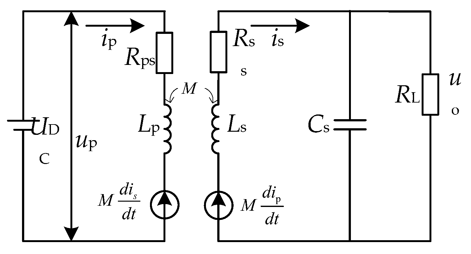
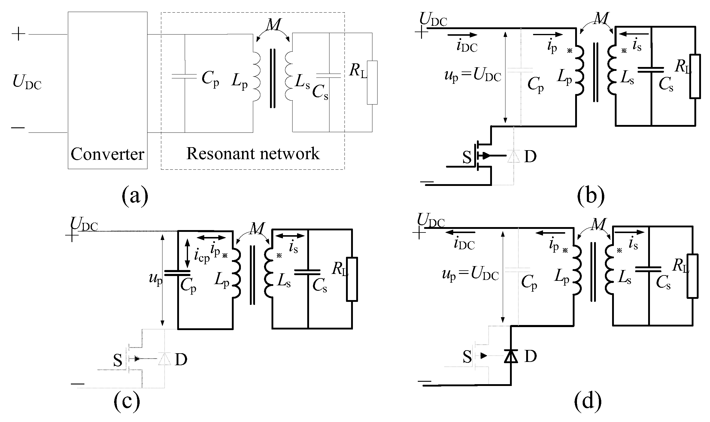
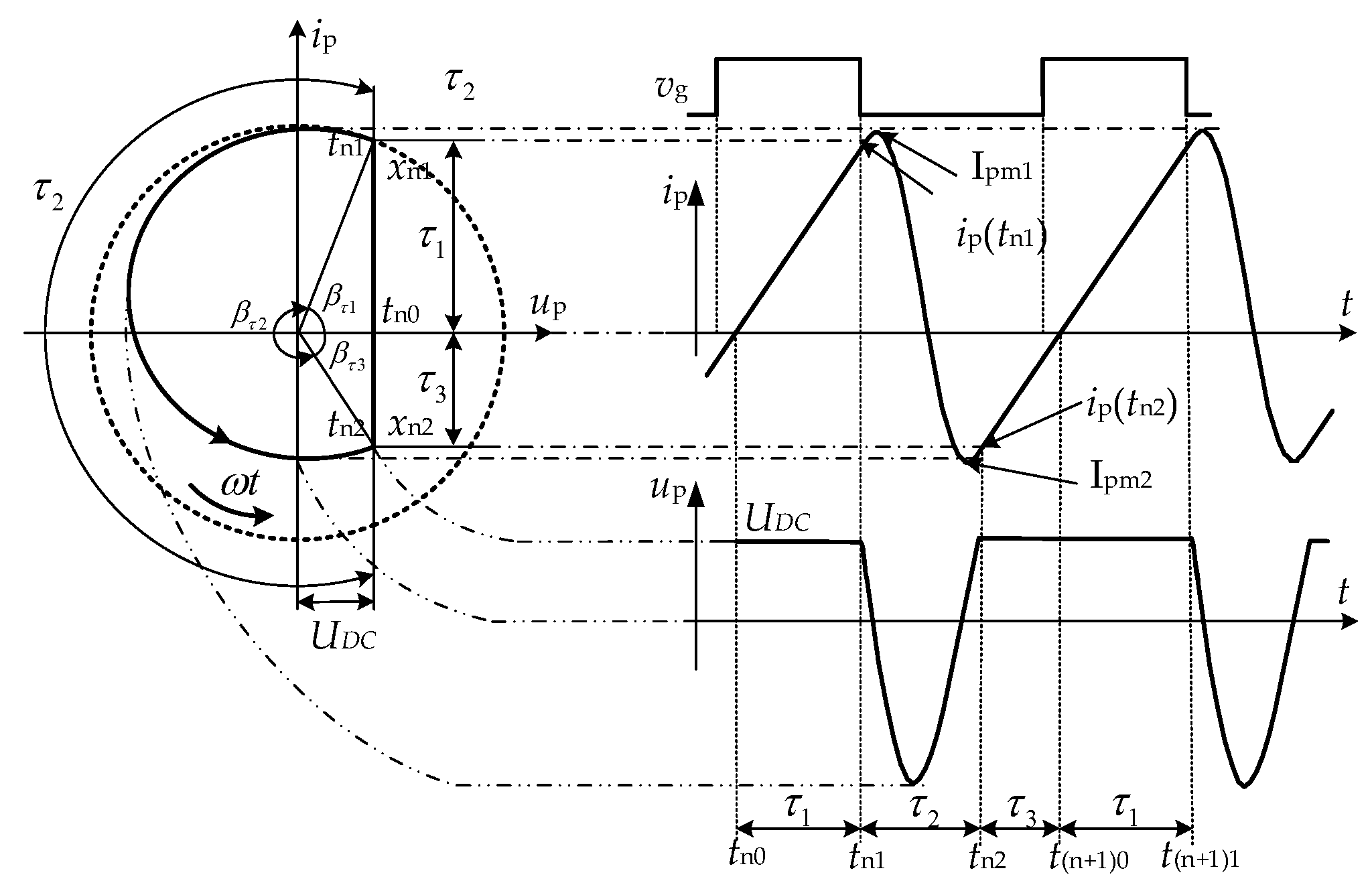
2. Variable Structure Analysis of an IPT System
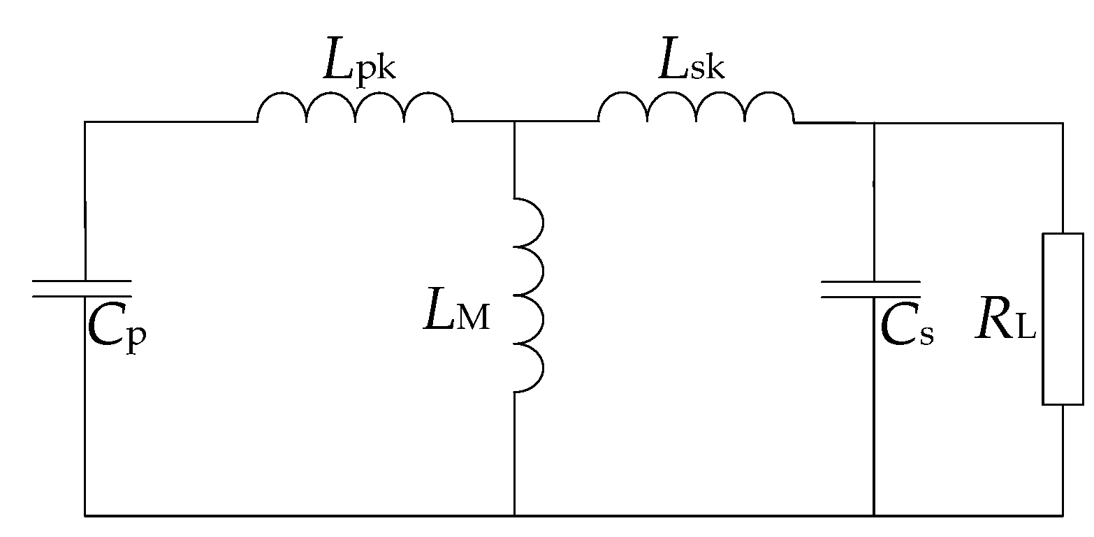
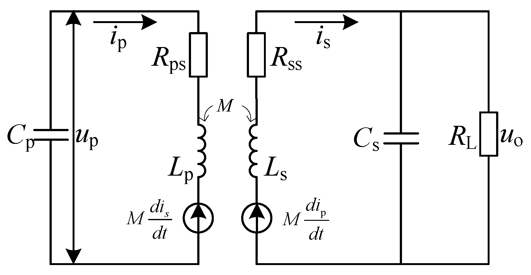
3. Mathematical Model
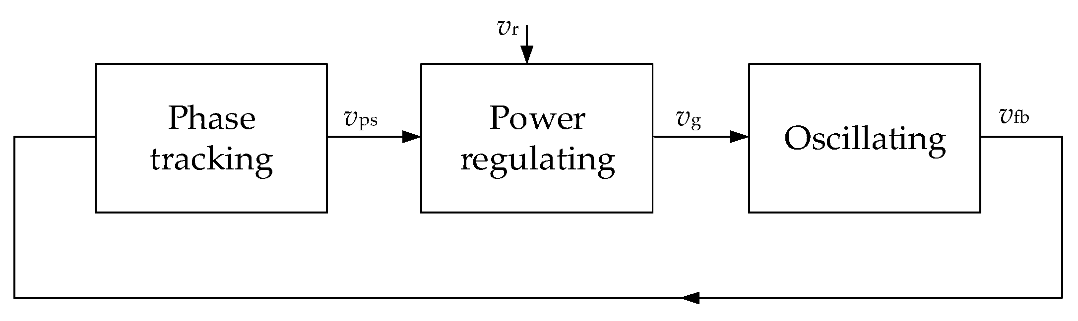
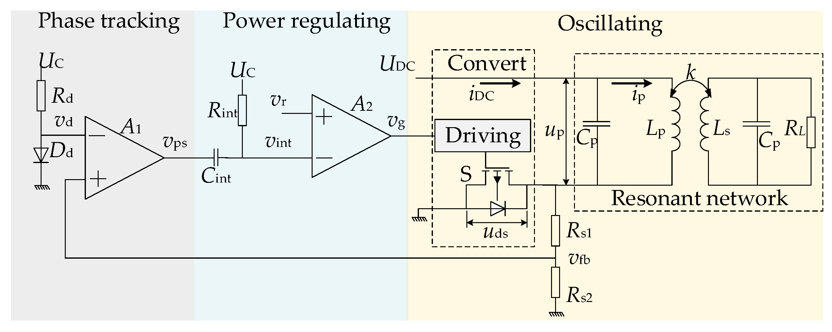
4. Control Method
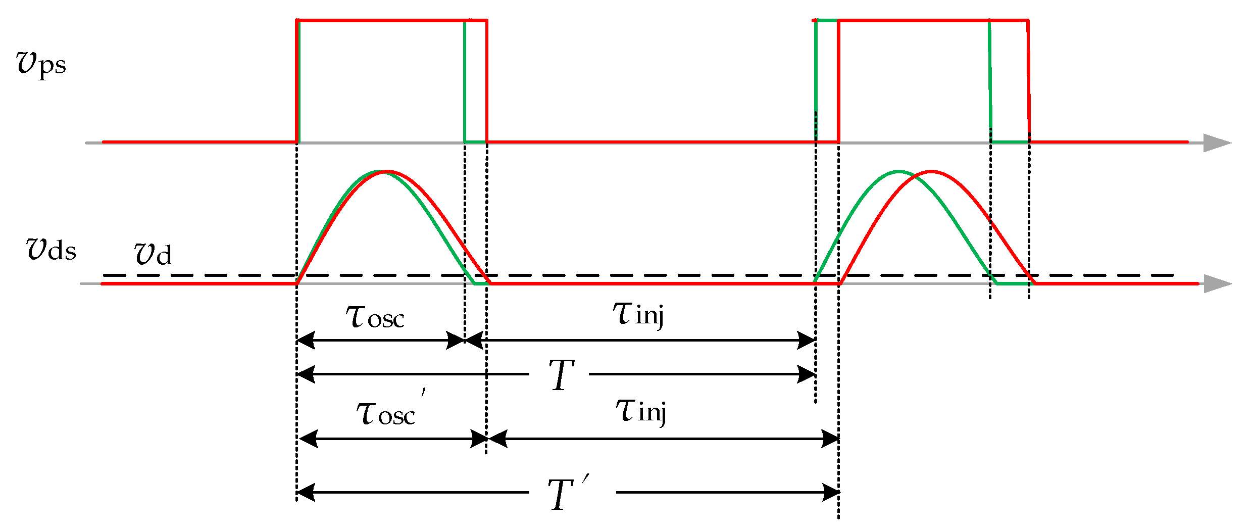
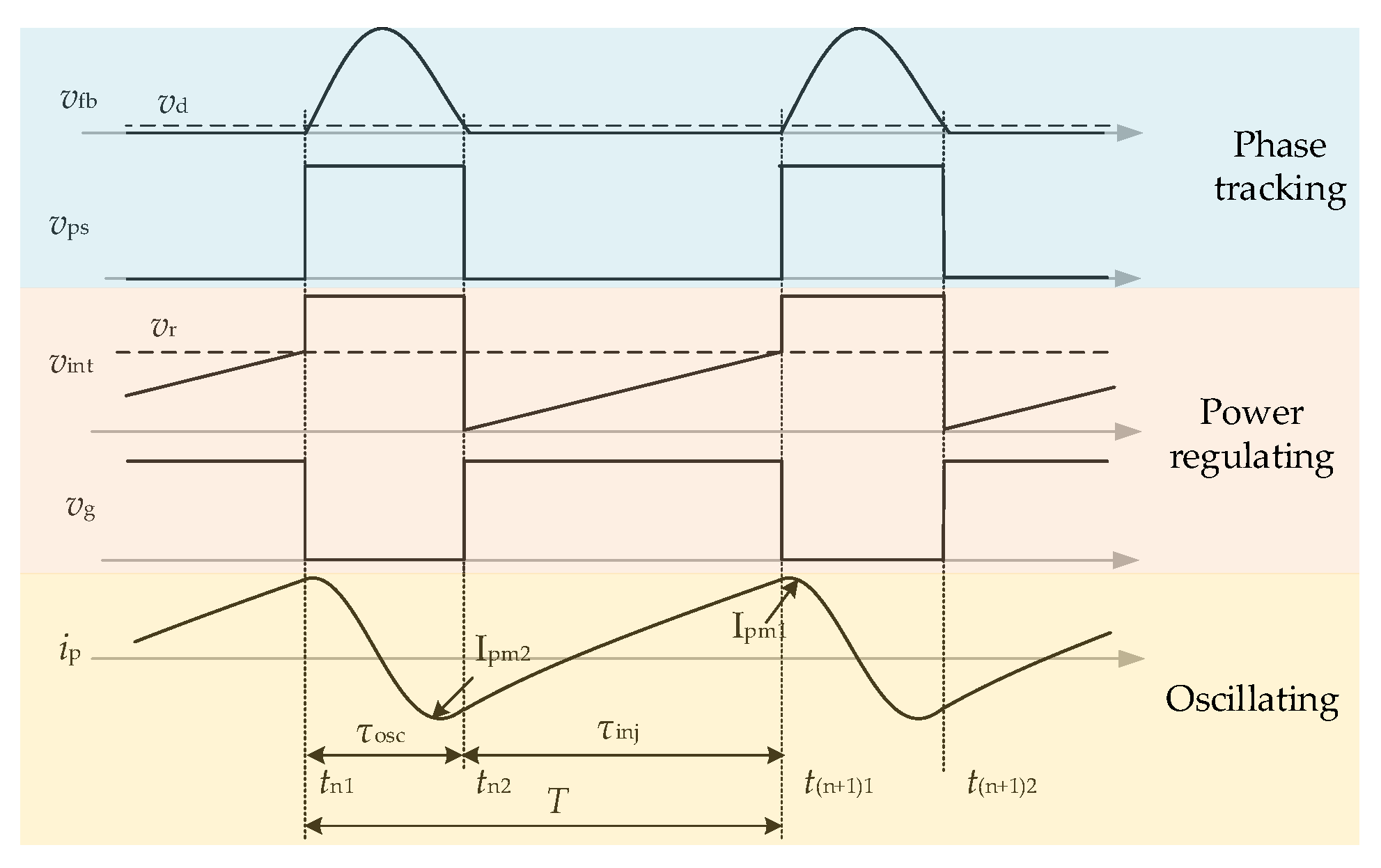
4.1. The Oscillating Unit
4.2. Phase Tracking Unit
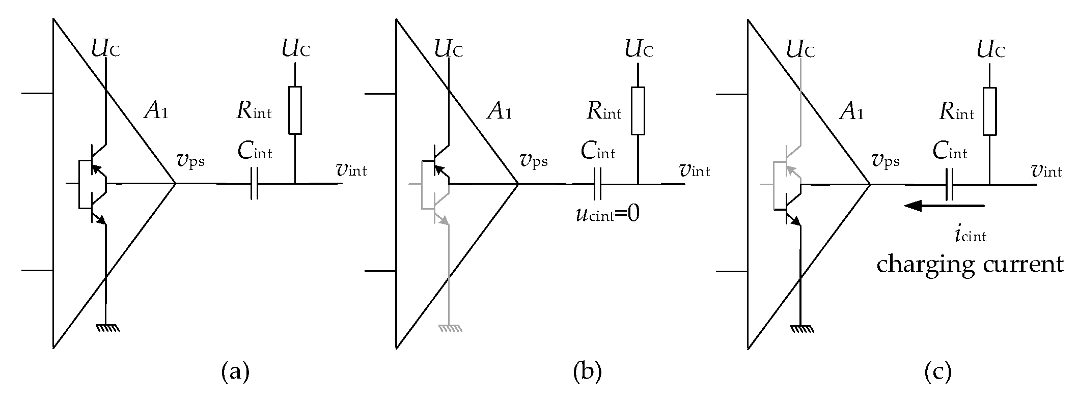
4.3. Power Injecting Unit
- (1)
- When vps is at a high level, the upper switch of the push–pull structure is turned on, as depicted in Figure 13b. In this case, both ends of the capacitor Cint are connected to Uc, resulting in zero voltage across Cint. Consequently, the integrator ceases its operation, and the integrator output vint = Uc.
- (2)
- As vps is lowered, the lower switch of the push–pull structure is activated, as shown in Figure 13c. In this scenario, the input of the integrator is connected to the ground, initiating the charging of capacitor Cint through Rint by Uc. As a result, the output of the integrator, vint, begins to increase from zero. The expression for vint can be represented as follows:
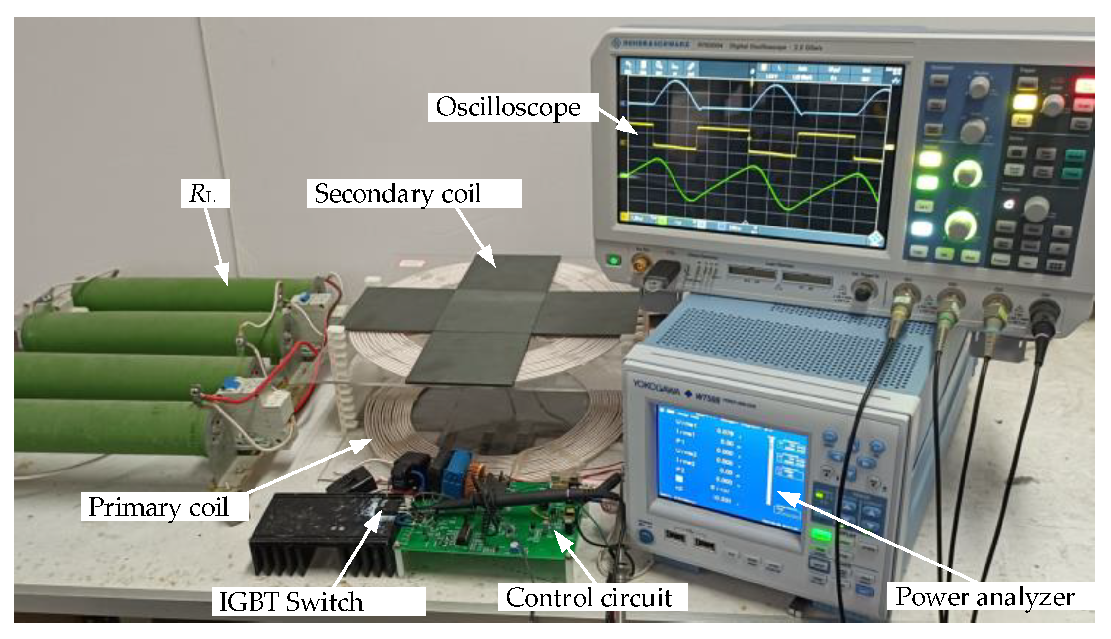
5. Validate Prototypes and Experiment
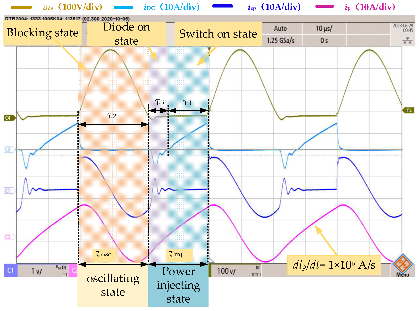
5.1. Self-Oscillation Characteristic Verification
- (1)
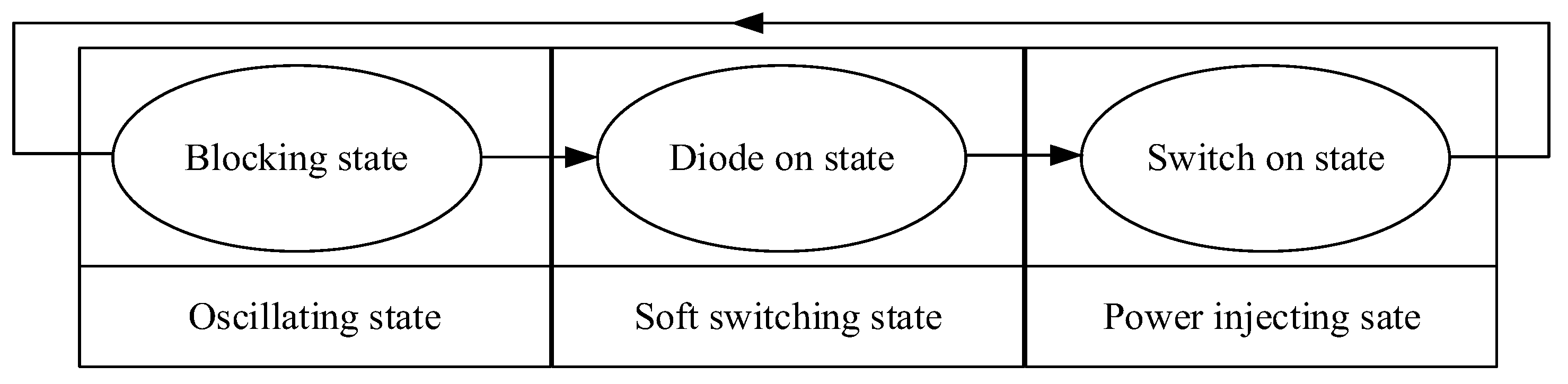
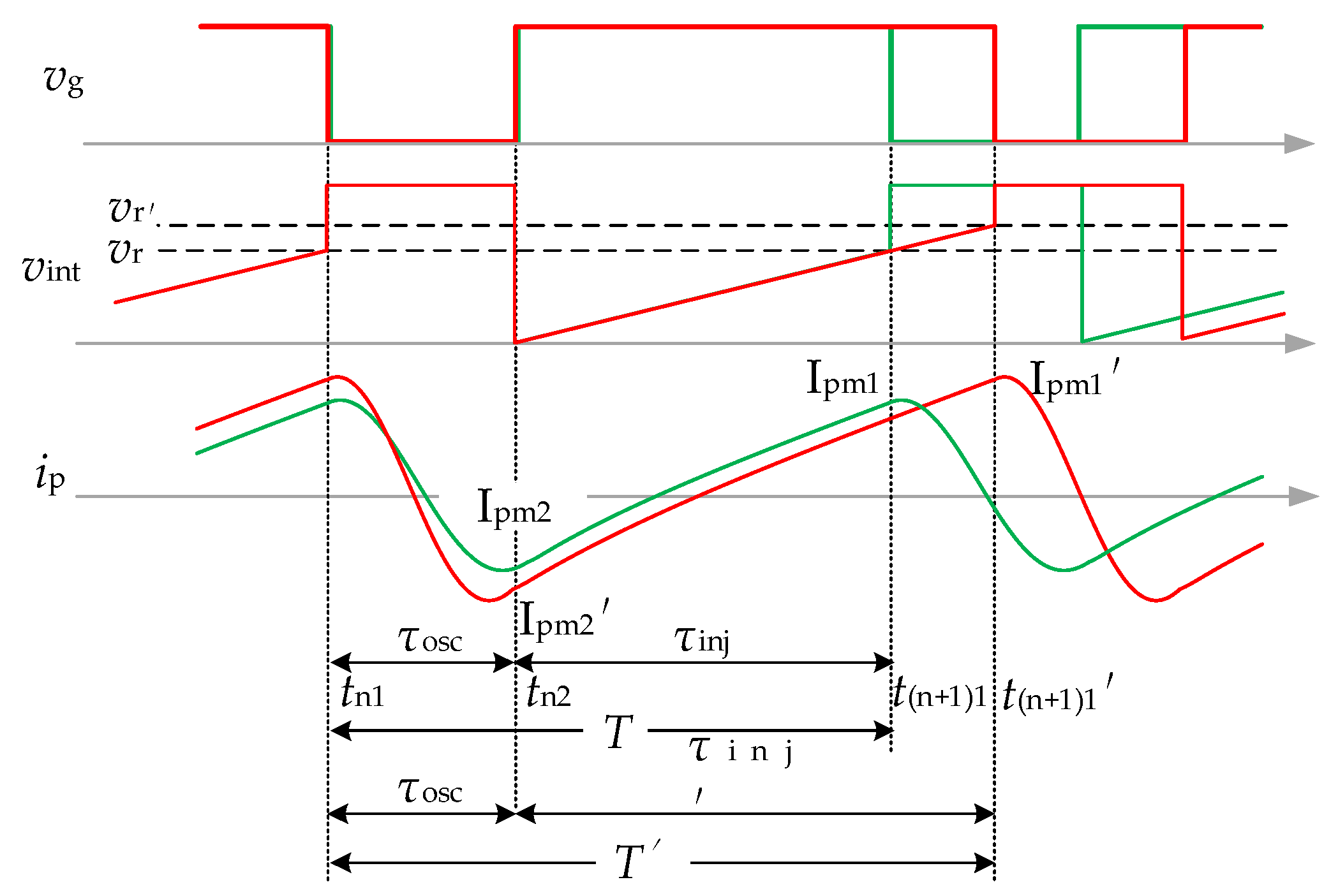
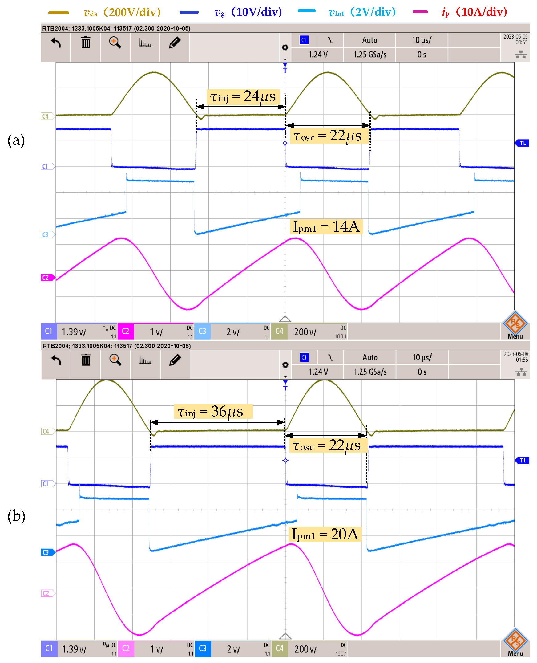
- The system operates in a closed loop, following the sequence of the blocking (self-oscillating) state, τ2, the diode-on state τ3, and the switch-on state τ1, as described in Figure 4. This demonstrates that the system is capable of self-oscillation, with the oscillation process repeating in the oscillating state, τosc, and the power injecting state, τinj.
- (2)
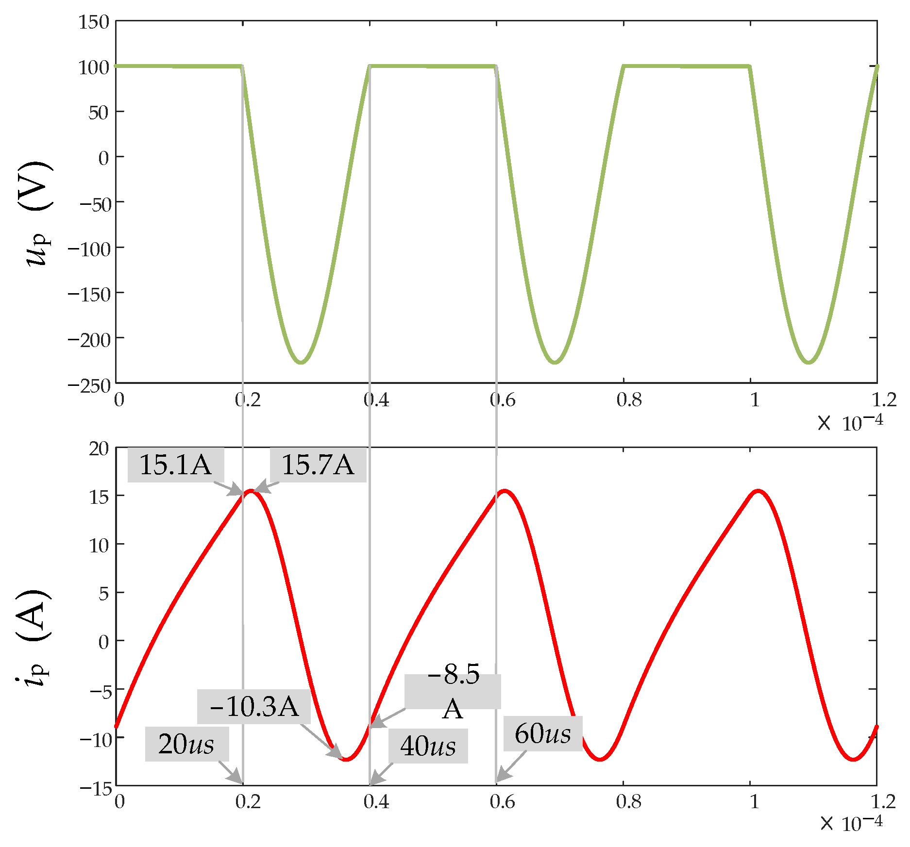
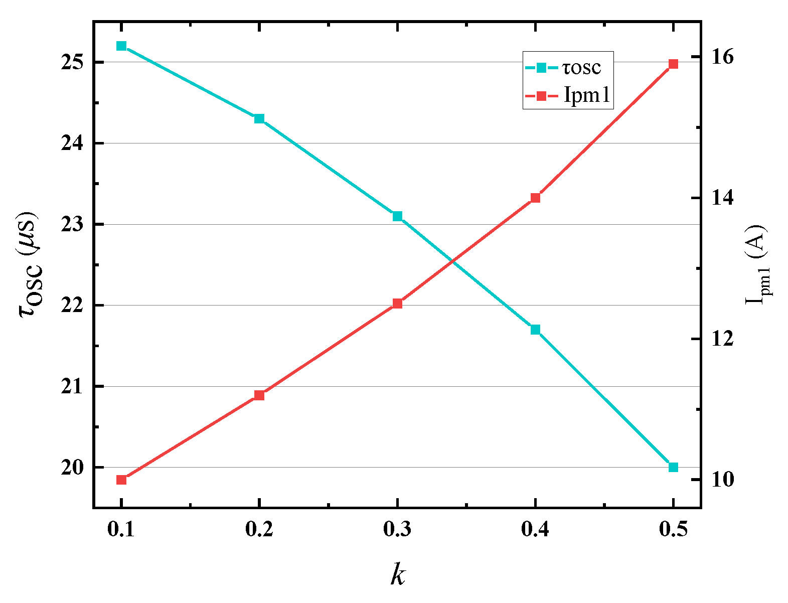
- During the oscillating state, iDC is equal to zero, indicating that the oscillating network is isolated from UDC. The capacitor Cp and inductor Lp form a resonant tank and initiate oscillation. The capacitor voltage, vds (up), capacitor current, icp, and the inductor current, ip, exhibit sinusoidal changes, with icp and ip being equal. Clearly, the oscillation is sustained for less than one cycle. The oscillation state duration τosc being 22 μs, slightly larger than the simulation results shown in Figure 8. This deviation may be caused by the deviation of component parameters.
- (3)
- In the diode-on state, iDC is negative, indicating that the current ip flows back to UDC through the diode. In the switch-on state, iDC is positive, indicating that UDC injects a current into the inductor Lp. Combining the diode-on state, τ3, and the switch-on state, τ1, into the power injecting state τinj, it can be observed that during the power injecting state, ip linearly increases from negative to positive with a rise slope of 1 × 10⁶ A/s, consistent with the calculated result from Equation (1). Additionally, the capacitor current, icp, is zero during the power injecting state, implying that the capacitor voltage is clamped to UDC during these two states.
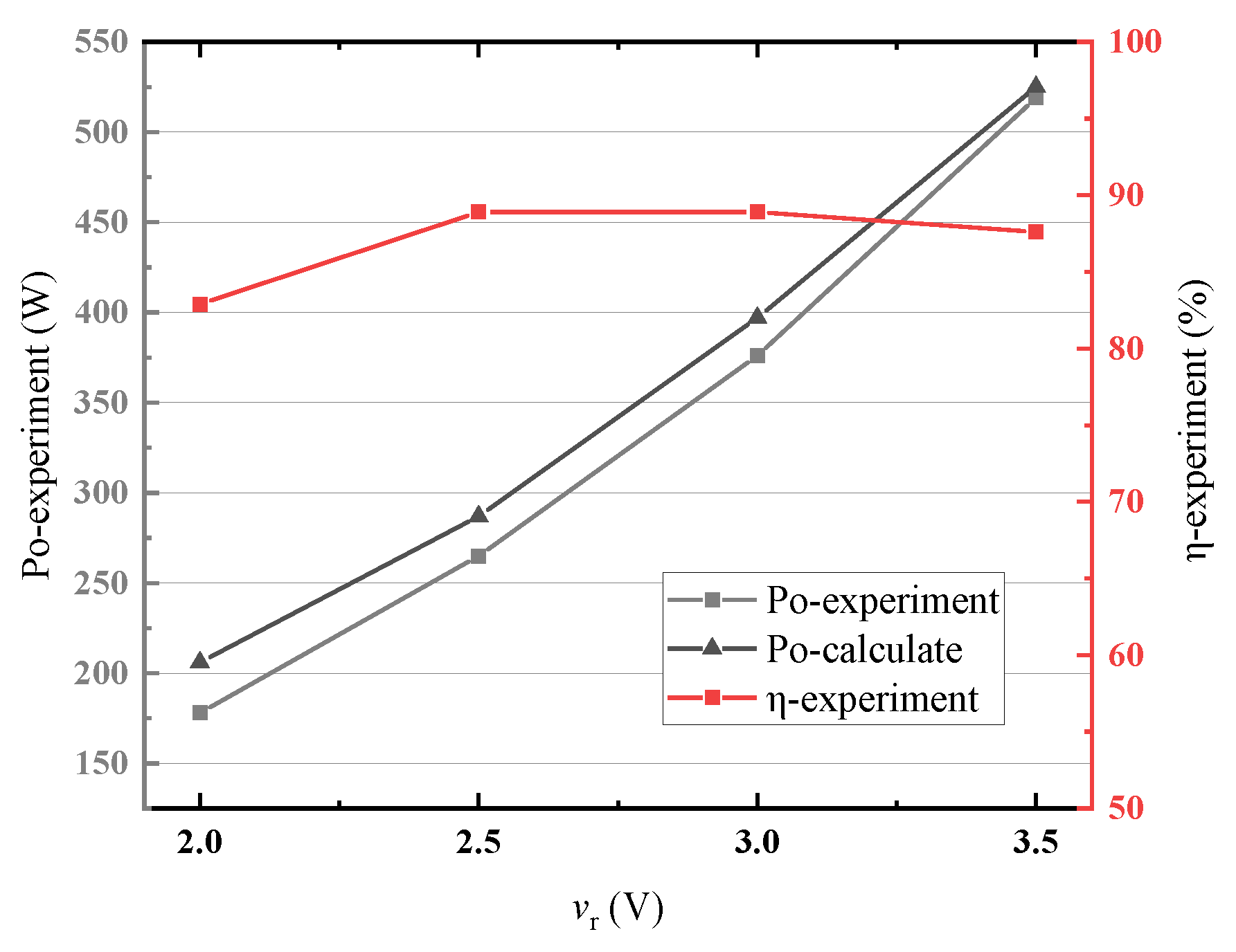
5.2. Power Regulating Verification
- (1)
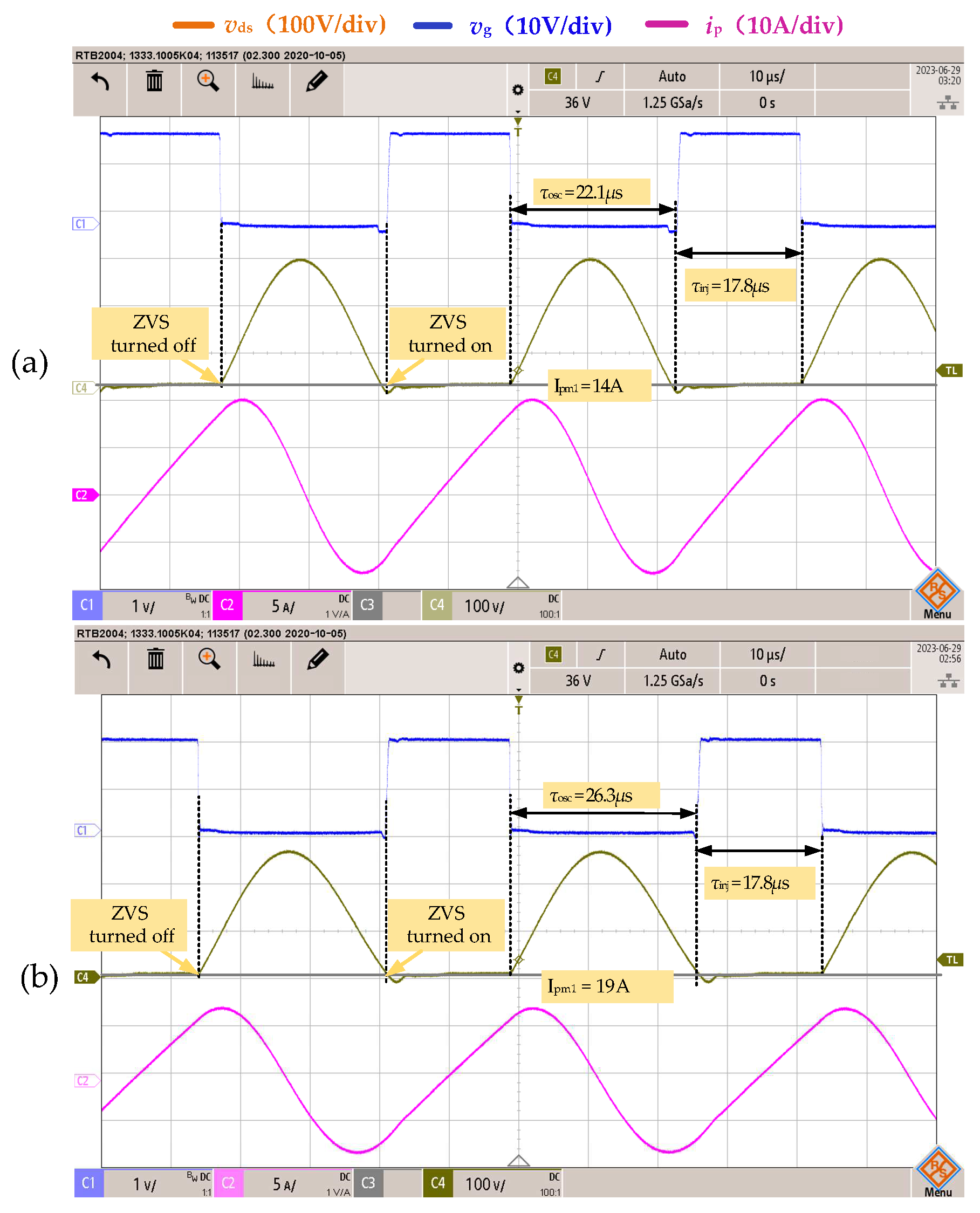
- The experimental curves are exactly the same as the principle curves shown in Figure 16, which indicates that the system can realize self-oscillation according to the order of the self-oscillating state and power injecting state.
- (2)
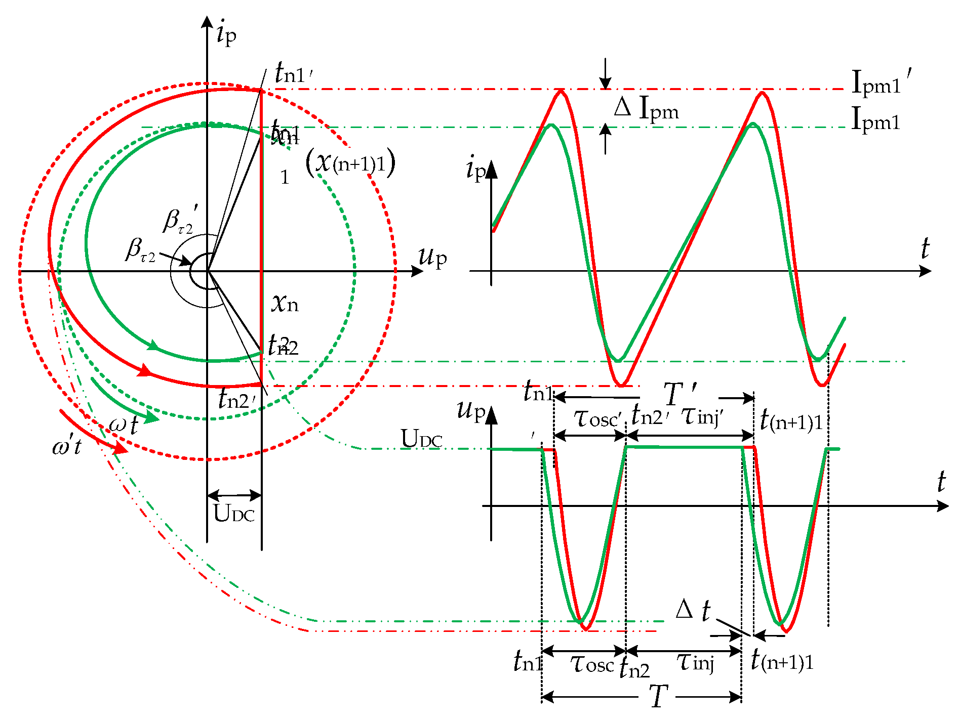
- The power injecting state duration can only be controlled by the control variable vr. The comparison between (a) and (b) shows that when vr increases from 2.5 V to 3.5 V, the power injection duration τinj increases from 24 μs to 36 μs, and the amplitude Ipm1 of the current ip increases from 14 A to 20 A, indicating that the power can be adjusted by controlling vr.
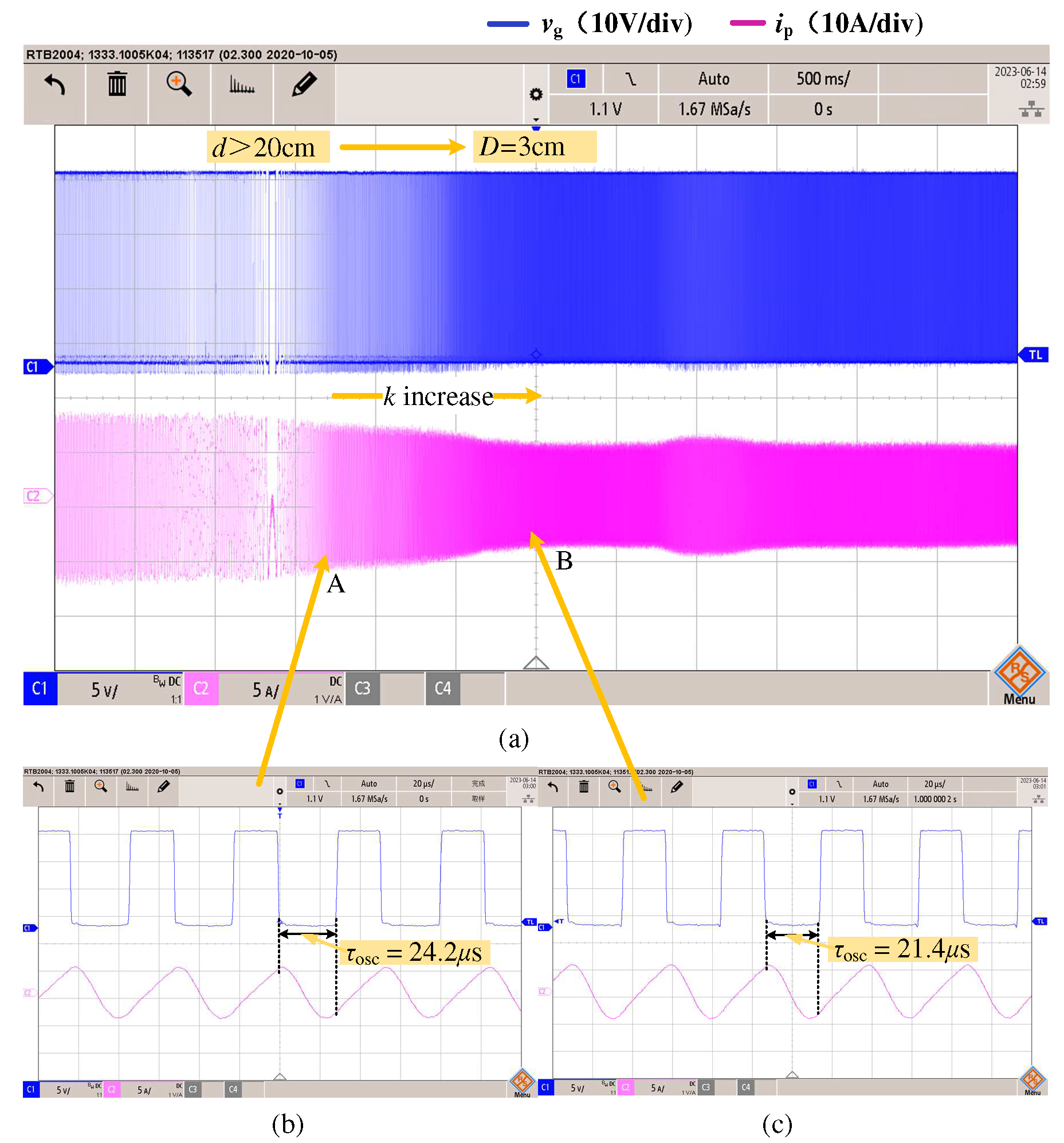
5.3. Phase Tracking and Soft Switch Condition Verification
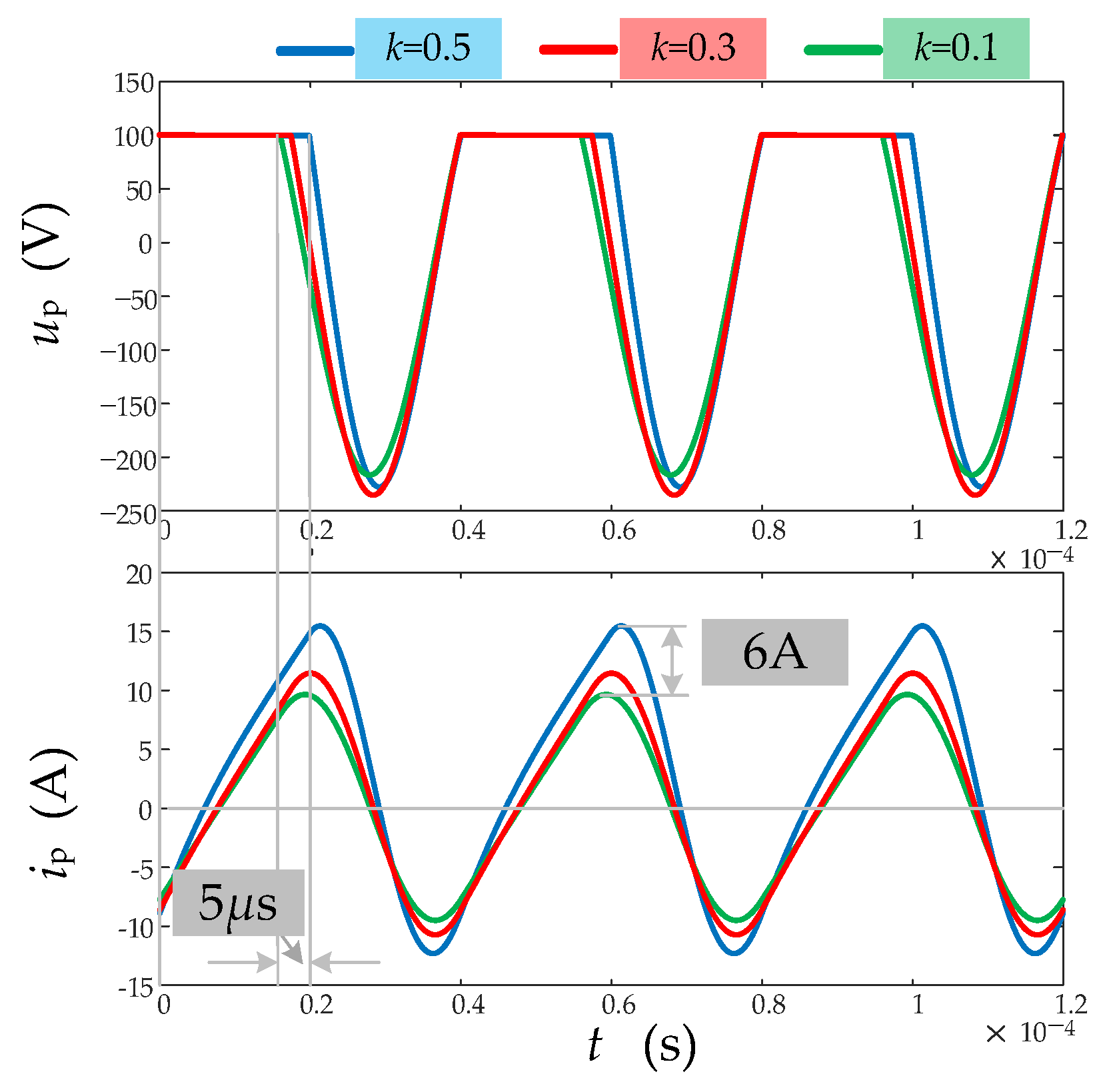
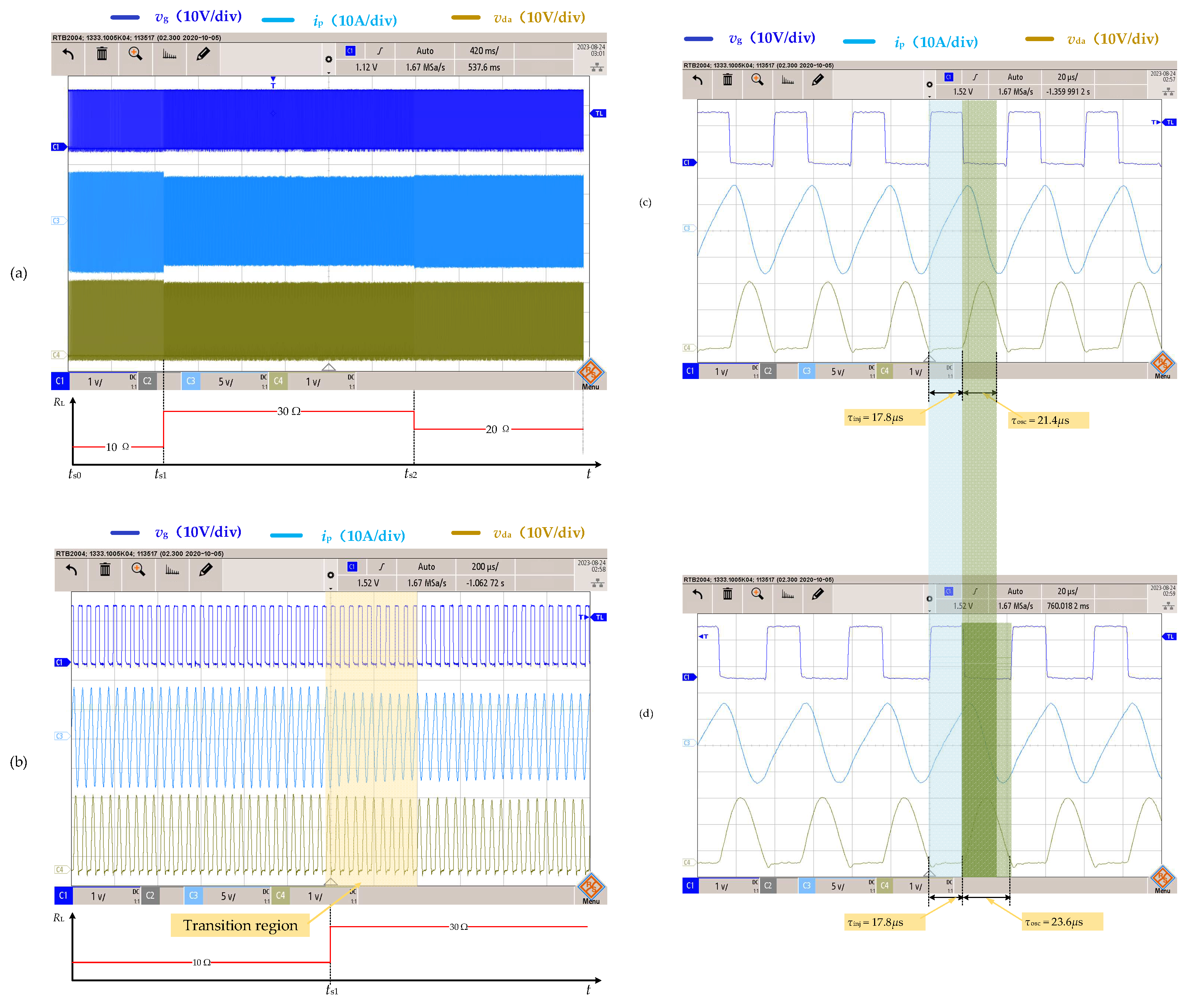
5.4. Dynamic Characteristics Verification
6. Conclusions
- (1)
- The working process of a converter can be divided into three distinct states: the switch-on state, blocking state, and diode-on state. This division allows for decoupling of the resonant network from the converter. By combining the switch-on state and diode-on state into power injecting state, and considering the blocking state as oscillating state, the working process of an IPT system consists of two state sequences: power injecting and oscillating states. By controlling the duration of the power injecting state, the output power can be adjusted independently. Furthermore, by detecting the duration of the self-oscillating state, changes in frequency can be accurately tracked and compensated for. The diode-on state’s soft switching characteristics enable a smooth transition between the power injecting and oscillating states.
- (2)
- The proposed phase-closed loop, comprising the phase tracking unit, power regulating unit, and oscillating unit, proves to be effective. This closed loop enables the system to switch between the power injecting state and oscillating state under soft switching condition.
- (3)
- Experimental results demonstrate that the phase tracking unit accurately tracks frequency drift caused by system parameters, indicating excellent frequency tracking characteristics. Furthermore, the experiments show that the system exhibits robust frequency tracking, even under conditions of a large coupling coefficient and maximum speed change.
- (4)
- The proposed power control method utilizing an integrator is proved to be effective. With the power injecting process decoupling from the oscillating process, power regulation only requires manipulation of the control variable vr. The experimental results indicate that the output power monotonically increases with the control variables vr. This power regulation characteristic simplifies and enhances the reliability of designing an IPT system control strategy.
Author Contributions
Funding
Data Availability Statement
Conflicts of Interest
Nomenclature
| IPT | Inductive Power Transfer |
| ZPA | Zero Phase Angle |
| PLL | Phase-Locked Loop |
| ZVS | Zero Voltage Switch |
| UDC | Bus-bar voltage |
| Lp | Primary inductance |
| Ls | Secondary inductance |
| Lpk | Primary leakage inductance |
| Lsk | Secondary leakage inductance |
| M | Mutual inductance |
| LM | mutual inductance |
| k | Coupling coefficient |
| KE | Primary current slop |
| Cp | Primary capacitance |
| Cs | Secondary capacitance |
| Cint | Integrating capacitance of power injecting unit |
| RL | Equivalent load |
| Rps | Primary loss resistance |
| Rss | Secondary loss resistance |
| Rint | Integrating resistance of power injecting unit |
| A1 | Phase tracking unit comparator |
| A2 | Power regulating unit comparator |
| S | Power switch |
| ip | Primary inductor current |
| is | Secondary inductor current |
| up | Primary capacitor voltage |
| uo | Output voltage |
| uds | Voltage across switch S |
| vg | Control signal of switch |
| vfb | Feedback signals from the oscillating network |
| vd | Comparison threshold of Phase tracking unit |
| vps | Output voltage of Phase tracking unit |
| vint | Integrator output voltage |
| vr | System power control voltage |
| τ1 | Duration of switch-on state |
| τ2 | Duration of blocking state |
| τ3 | Duration of diode-on state |
| τinj | Duration of power injecting state |
| τosc | Duration of self-oscillating state |
| ω | Self-oscillating angular frequency |
| βτ1 | Phase angle occupied by switch-on state |
| βτ2 | Phase angle occupied by blocking state |
| βτ3 | Phase angle occupied by diode-on state |
| P0 | Output power |
| Ipm1/IPm2 | Maximum value of primary current, ip |
| T | Energy transfer period |
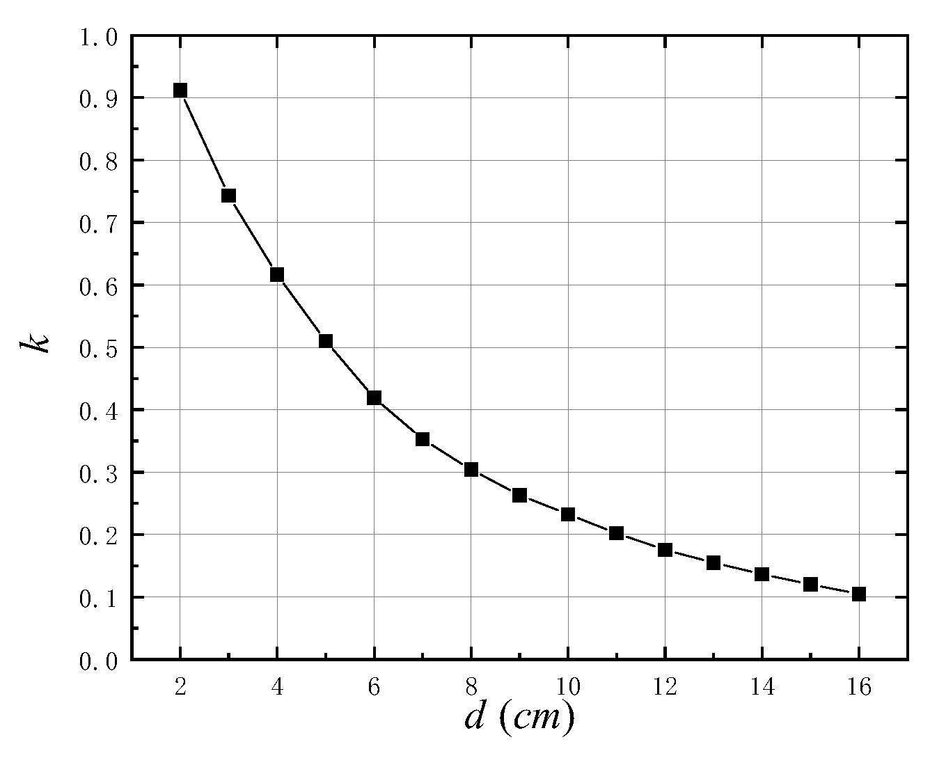
| d | The air gap between the two coils |
| Idc | Bus current |
References
- Liu, H.; Shao, Q.; Fang, X. Modeling and Optimization of Class-E Amplifier at Subnominal Condition in a Wireless Power Transfer System for Biomedical Implants. IEEE Trans. Biomed. Circuits Syst. 2016, 11, 35–43. [Google Scholar] [CrossRef]
- Ruffo, R.; Cirimele, V.; Diana, M.; Khalilian, M.; La Ganga, A.; Guglielmi, P. Sensorless control of the charging process of a dynamic inductive power transfer system with interleaved nine-phase boost converter. IEEE Trans. Ind. Electron. 2018, 65, 7630–7639. [Google Scholar] [CrossRef]
- Zhao, L.; Thrimawithana, D.J.; Madawala, U.K.; Hu, A.P. A Push–Pull Parallel Resonant Converter-Based Bidirectional IPT System. IEEE Trans. Power Electron. 2019, 35, 2659–2667. [Google Scholar] [CrossRef]
- Wang, C.S.; Covic, G.A.; Stielau, O.H. Investigating an LCL load resonant inverter for inductive power transfer applications. IEEE Trans. Power Electron. 2004, 19, 995–1002. [Google Scholar] [CrossRef]
- Zhang, W.; Wong, S.-C.; Tse, C.K.; Chen, Q. Design for Efficiency Optimization and Voltage Controllability of Series–Series Compensated Inductive Power Transfer Systems. IEEE Trans. Power Electron. 2013, 29, 191–200. [Google Scholar] [CrossRef]
- Stielau, O.H.; Covic, G.A. Design of loosely coupled inductive power transfer systems. In Proceedings of the 2000 International Conference on Power System Technology, Perth, WA, Australia, 4–7 December 2000. [Google Scholar] [CrossRef]
- Mohamed, A.A.S.; Berzoy, A.; de Almeida, F.G.N.; Mohammed, O. Modeling and Assessment Analysis of Various Compensation Topologies in Bidirectional IWPT System for EV Applications. IEEE Trans. Ind. Appl. 2017, 53, 4973–4984. [Google Scholar] [CrossRef]
- Shevchenko, V.; Husev, O.; Strzelecki, R.; Pakhaliuk, B.; Poliakov, N.; Strzelecka, N. Compensation Topologies in IPT Systems: Standards, Requirements, Classification, Analysis, Comparison and Application. IEEE Access 2021, 7, 120559–120580. [Google Scholar] [CrossRef]
- Houran, M.A.; Yang, X.; Chen, W. Magnetically Coupled Resonance WPT: Review of Compensation Topologies, Resonator Structures with Misalignment, and EMI Diagnostics. Electronics 2018, 7, 296. [Google Scholar] [CrossRef]
- Mohamed, A.A.S.; Shaier, A.A.; Metwally, H.; Selem, S.I. An Overview of Dynamic Inductive Charging for Electric Vehicles. Energies 2022, 15, 5613. [Google Scholar] [CrossRef]
- Wang, C.S.; Covic, G.A.; Stielau, O.H. Power transfer capability and bifurcation phenomena of loosely coupled inductive power transfer systems. IEEE Trans. Ind. Electron. 2004, 51, 148–157. [Google Scholar] [CrossRef]
- Villa, J.L.; Sallan, J.; Osorio, J.F.S.; Llombart, A. High-Misalignment Tolerant Compensation Topology for ICPT Systems. IEEE Trans. Ind. Electron. 2011, 59, 945–951. [Google Scholar] [CrossRef]
- Fotopoulou, K.; Flynn, B.W. Wireless Power Transfer in Loosely Coupled Links: Coil Misalignment Model. IEEE Trans. Magn. 2011, 47, 416–430. [Google Scholar] [CrossRef]
- Su, Y.-G.; Zhang, H.-Y.; Wang, Z.-H.; Hu, A.P.; Chen, L.; Sun, Y. Steady-State Load Identification Method of Inductive Power Transfer System Based on Switching Capacitors. IEEE Trans. Power Electron. 2015, 30, 6349–6355. [Google Scholar] [CrossRef]
- Li, Y.; Dong, W.; Yang, Q.; Jiang, S.; Ni, X.; Liu, J. Automatic Impedance Matching Method with Adaptive Network Based Fuzzy Inference System for WPT. IEEE Trans. Ind. Inform. 2020, 16, 1076–1085. [Google Scholar] [CrossRef]
- Luo, Y.; Yang, Y.; Chen, S.; Wen, X. A Frequency-Tracking and Impedance-Matching Combined System for Robust Wireless Power Transfer. Int. J. Antennas Propag. 2017, 2017, 5719835. [Google Scholar] [CrossRef]
- Zahiribarsari, V.; Thrimawithana, D.J.; Covic, G.A. An Inductive Coupler Array for In-Motion Wireless Charging of Electric Vehicles. IEEE Trans. Power Electron. 2021, 36, 9854–9863. [Google Scholar]
- Gati, E.; Kampitsis, G.; Manias, S. Variable Frequency Controller for Inductive Power Transfer in Dynamic Conditions. IEEE Trans. Power Electron. 2016, 32, 1684–1696. [Google Scholar] [CrossRef]
- Matysik, J.T. The Current and Voltage Phase Shift Regulation in Resonant Converters with Integration Control. IEEE Trans. Ind. Electron. 2007, 54, 1240–1242. [Google Scholar] [CrossRef]
- Kim, D.H.; Kim, M.S.; Kim, H.J. Frequency-Tracking Algorithm Based on SOGI-FLL for Wireless Power Transfer System to Operate ZPA Region. Electronics 2020, 9, 1303. [Google Scholar] [CrossRef]
- Hong, J.; Guan, M.; Lin, Z.; Fang, Q.; Wu, W.; Chen, W. Series-Series/Series Compensated Inductive Power Transmission System with Symmetrical Half-Bridge Resonant Converter: Design, Analysis, and Experimental Assessment. Energies 2019, 12, 2268. [Google Scholar] [CrossRef]
- Namadmalan, A. Self-Oscillating Tuning Loops for Series Resonant Inductive Power Transfer Systems. IEEE Trans. Power Electron. 2016, 31, 7320–7327. [Google Scholar] [CrossRef]
- Xu, L.; Chen, Q.; Ren, X.; Wong, S.; Tse, C. Self-Oscillating Resonant Converter with Contactless Power Transfer and Integrated Current Sensing Transformer. IEEE Trans. Power Electron. 2016, 32, 4839–4851. [Google Scholar] [CrossRef]
- Namadmalan, A. Self-Oscillating Pulse Width Modulation for Inductive Power Transfer Systems. IEEE J. Emerg. Sel. Top. Power Electron. 2019, 8, 1813–1820. [Google Scholar] [CrossRef]
- Wei, Z.; Zhang, B.; Lin, S.; Wang, C. A Self-Oscillation WPT System with High Misalignment Tolerance. IEEE Trans. Power Electron. 2023, 39, 1870–1887. [Google Scholar] [CrossRef]
- Li, H.; Li, J.; Wang, K.; Chen, W.; Yang, X. A Maximum Efficiency Point Tracking Control Scheme for Wireless Power Transfer Systems Using Magnetic Resonant Coupling. IEEE Trans. Power Electron. 2015, 30, 3998–4008. [Google Scholar] [CrossRef]
- Miller, J.M.; Onar, O.C.; Chinthavali, M. Primary-Side Power Flow Control of Wireless Power Transfer for Electric Vehicle Charging. IEEE J. Emerg. Sel. Top. Power Electron. 2014, 3, 147–162. [Google Scholar] [CrossRef]
- Hu, H.; Cai, T.; Duan, S.; Zhang, X.; Niu, J.; Feng, H. An Optimal Variable Frequency Phase Shift Control Strategy for ZVS Operation within Wide Power Range in IPT Systems. IEEE Trans. Power Electron. 2019, 35, 5517–5530. [Google Scholar] [CrossRef]
- Berger, A.; Agostinelli, M.; Vesti, S.; Oliver, J.A.; Cobos, J.A.; Huemer, M. A Wireless Charging System Applying Phase-Shift and Amplitude Control to Maximize Efficiency and Extractable Power. IEEE Trans. Power Electron. 2015, 30, 6338–6348. [Google Scholar] [CrossRef]
- Wu, W.; Luo, D.; Hong, J.; Tang, Z.; Chen, W. A Six-Switch Mode Decoupled Wireless Power Transfer System with Dynamic Parameter Self-Adaption. Electronics 2023, 12, 2314. [Google Scholar] [CrossRef]
- Chen, L.; Hong, J.; Lin, Z.; Luo, D.; Guan, M.; Chen, W. A Converter with Automatic Stage Transition Control for Inductive Power Transfer. Energies 2020, 13, 5268. [Google Scholar] [CrossRef]
- Dranga, O.; Buti, B.; Nagy, I.; Funato, H. Stability analysis of nonlinear power electronic systems utilizing periodicity and introducing auxiliary state vector. IEEE Trans. Circuits Syst. I Regul. Pap. 2005, 52, 168–178. [Google Scholar] [CrossRef]
- Buti, B.; Nagy, I.; Ohsaki, H.; Masada, E. Novel Approach in Stability Analysis Presented in Controlled Boost Converter. In Proceedings of the Power Conversion Conference, Nagoya, Japan, 2–5 April 2007; IEEE: Piscataway, NJ, USA, 2007; pp. 581–587. [Google Scholar]


| Ref. | Compensation Network | Closed-Loop | Feedback Signal | Resonant Mode | Coupling between Converter and Network | Power Control Strategy |
|---|---|---|---|---|---|---|
| [20] | S-S | Yes | Primary side Current | Perfect resonance | Strong | — |
| [23] | S-S | Yes | Primary side Current | Perfect resonance | Strong | Regulating phase |
| [25] | S-CC | Yes | Current from current transformer | Perfect resonance | Strong | Regulating phase |
| [26] | S-S | Yes | Load voltage | Perfect resonance | Strong | Additional converter |
| [28] | LCC-S | Yes | Load voltage and current | Perfect resonance | Strong | Regulating phase |
| [31] | P-S | No | — | quasi-resonant | No | Regulating the duration of energy injection state |
| This work | P-P | Yes | Voltage from primary side | quasi-resonant | No | Regulating the duration of energy injection state |
| Parameter | Design Value | Parameter | Design Value |
|---|---|---|---|
| UDC | 100 V | Lp, Ls | 100 μH, 100 μH |
| M | 50 μH | Cp, Cs | 0.3 μF, 0.3 μF |
| Rps, Rss | 0.07 Ω, 0.07 Ω | T | 40 μs |
| Parameter | Value | Parameter | Value |
|---|---|---|---|
| UDC, Uc | 100–200 V, 5 V | Comparator | LM339 |
| Rint, Cint | 50 k, 20 nF | Rd, Dd | 1 k, 1N4148 |
| IGBT | H30R1602 | RL | 10–50 Ω |
Disclaimer/Publisher’s Note: The statements, opinions and data contained in all publications are solely those of the individual author(s) and contributor(s) and not of MDPI and/or the editor(s). MDPI and/or the editor(s) disclaim responsibility for any injury to people or property resulting from any ideas, methods, instructions or products referred to in the content. |
© 2024 by the authors. Licensee MDPI, Basel, Switzerland. This article is an open access article distributed under the terms and conditions of the Creative Commons Attribution (CC BY) license (https://creativecommons.org/licenses/by/4.0/).
Share and Cite
Chen, L.; Luo, D.; Hong, J.; Guan, M.; Chen, W. Self-Oscillating Converter Based on Phase Tracking Closed Loop for a Dynamic IPT System. Energies 2024, 17, 1814. https://doi.org/10.3390/en17081814
Chen L, Luo D, Hong J, Guan M, Chen W. Self-Oscillating Converter Based on Phase Tracking Closed Loop for a Dynamic IPT System. Energies. 2024; 17(8):1814. https://doi.org/10.3390/en17081814
Chicago/Turabian StyleChen, Lin, Daqing Luo, Jianfeng Hong, Mingjie Guan, and Wenxiang Chen. 2024. "Self-Oscillating Converter Based on Phase Tracking Closed Loop for a Dynamic IPT System" Energies 17, no. 8: 1814. https://doi.org/10.3390/en17081814
APA StyleChen, L., Luo, D., Hong, J., Guan, M., & Chen, W. (2024). Self-Oscillating Converter Based on Phase Tracking Closed Loop for a Dynamic IPT System. Energies, 17(8), 1814. https://doi.org/10.3390/en17081814