Article

Compact Trap-Assisted-Tunneling Model for Line Tunneling Field-Effect-Transistor Devices

ICT & Robotics Engineering and IITC, Hankyong National University, Anseong 17579, Korea
*
Author to whom correspondence should be addressed.
Appl. Sci. 2020, 10(13), 4475; https://doi.org/10.3390/app10134475
Submission received: 25 May 2020 / Revised: 24 June 2020 / Accepted: 24 June 2020 / Published: 28 June 2020
(This article belongs to the Special Issue Device Modeling for TCAD and Circuit Simulation)

Abstract

:
Trap-assisted-tunneling (TAT) is a well-documented source of severe subthreshold degradation in tunneling field-effect-transistors (TFET). However, the literature lacks in numerical or compact TAT models applied to TFET devices. This work presents a compact formulation of the Schenk TAT model that is used to fit experimental drain-source current (Ids) versus gate-source voltage (Vgs) data of an L-shaped and line tunneling type TFET. The Schenk model incorporates material-dependent fundamental physical constants that play an important role in influencing the TAT generation (GTAT) including the lattice relaxation energy, Huang–Rhys factor, and the electro-optical frequency. This makes fitting any experimental data using the Schenk model physically relevant. The compact formulation of the Schenk TAT model involved solving the potential profile in the TFET and using that potential profile to calculate GTAT using the standard Schenk model. The GTAT was then approximated by the Gaussian distribution function for compact implementation. The model was compared against technology computer-aided design (TCAD) results and was found in reasonable agreement. The model was also used to fit an experimental device’s IdsVgs characteristics. The results, while not exactly fitting the experimental data, follow the general experimental IdsVgs trend reasonably well; the subthreshold slope was loosely similar to the experimental device. Additionally, the ON-current, especially to make a high drain-source bias model accurate, can be further improved by including effects such as electrostatic degradation and series resistance.

1. Introduction

With conventional complementary metal-oxide-semiconductor (CMOS) technology coming to the end of its life cycle owing to scaling limitations, there has been significant interest in the research and development of alternate technologies including tunneling field-effect-transistors (TFET) [1,2,3]. TFETs work on the principle of band-to-band-tunneling, and provide a significantly better subthreshold slope (SS) as compared to metal-oxide-semiconductor field-effect-transistor (MOSFET) devices, and its ON-current (ION) issue [4] can be augmented with the help of alternate designs, including the line tunneling type TFET or III–V material TFET. In theory, this makes the TFET an ideal candidate to replace the aging MOSFET.
However, there is one issue that continues to be the bottleneck in the practical realization of the TFET. TFETs are very sensitive to subthreshold degradation caused by trap states [5]. Trap states cause trap-assisted-tunneling (TAT); TAT is a phonon-assisted band-to-band tunneling current generation process aided by trap states and is known to cause significant subthreshold slope degradation in TFETs. To date, there is very limited work available in the literature on the modeling of TAT mechanisms. Sajjad et al. [6] developed a compact TAT model based on Hurkx’s TAT model [7]. However, Hurkx’s TAT model can be considered a first-order model; it lacks fundamental and microscopic physical parameters that play a critical role in influencing TAT current including the phonon energy and Huang Rhys factor [8], which is a measure of the electron–phonon coupling and the lattice relaxation energy [9]. This makes fitting any experimental data with the help of the Hurkx model very difficult and without any physical relevance. Furthermore, the Hurkx model is a piece-wise model with different equations for different trap energy levels (ET) [10]. This makes its compact implementation impractical. The Schenk model [11] on the other hand, offers a more microscopic approach to TAT modeling and is easy to implement numerically. The Schenk model has been used in studies investigating the role of TAT in TFET devices. However, there is no numerical or compact implementation of the Schenk model in the literature. This paper presents a simple Schenk–TAT compact model that is applied to fit the experimental drain–source current (Ids)–gate–source voltage (Vgs) data of a line tunneling type and L-shaped TFET (LTFET) device [12]. The model is discussed in Section 2, and the results are discussed in Section 3. The conclusion is presented in Section 4.

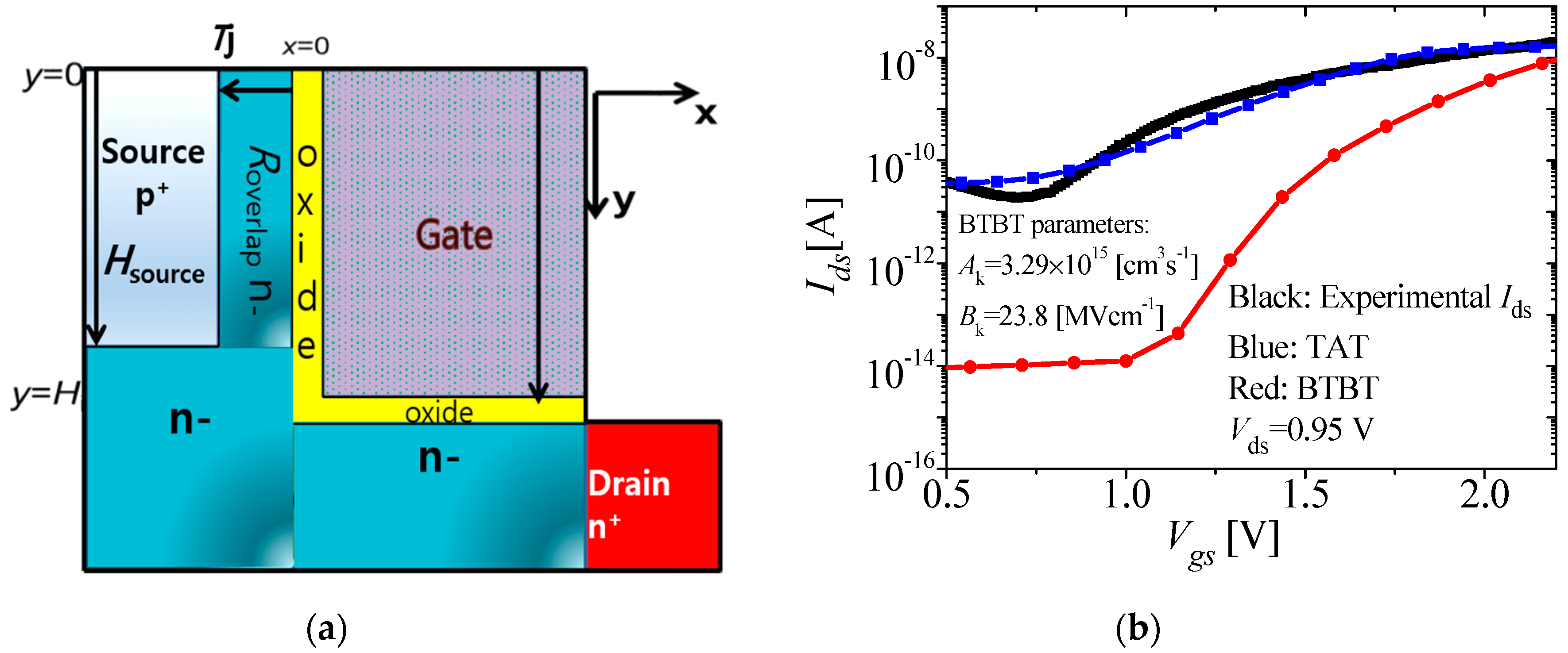
2. Model Presentation

Figure 1a shows the schematic of the LTFET [12]. The channel is sandwiched between the gate and source. The source with height Hsource = 70 nm is heavily p+ (1019 cm-3) doped with Hsource in the y direction, and the channel is n (1015 cm−3) doped. A part of the channel is also found underneath the source and does not overlap between the gate and source. This is termed as Rnonoverlap. The part of the channel that overlaps between the source and gate is termed as Roverlap and has a thickness Tj = 10 nm in the x direction and height (Hoverlap = Hsource = 70 nm [12,13]) in the y direction. The HfO2 gate dielectric is 2 nm thick (tox). The drain is heavily n+ doped (1019 cm−3).
Before delving into the details of the model, it is important to illustrate the different current mechanisms in line tunneling TFETs. There are three different current mechanisms including (1) 2D BTBT, (2) 1D BTBT, and (3) TAT. 2D BTBTs originate from the corner-effect present in line tunneling TFETs. Because of the corner shape present in line tunneling TFETs, where the source and channel meet, the electric field converges around the sharp source corner, and increases the potential in the area surrounding the corner region [14]. This increased potential causes a 2D BTBT. The threshold voltage of 2D BTBT is lower than that of a 1D BTBT. However, the threshold voltage of the TAT is lower than that of the 2D BTBT and, as a consequence, the TAT current is generated at a lower Vgs than both the 2D and 1D BTBT currents. This is summarized in Table 1. Details of the 1D and 2D BTBT mechanisms can be found in [15,16]. Depending on the number of traps, their energy level, density and whether the traps are bulk or interface traps, the TAT generated drain current can vary. In most cases, the TAT current dominates the low Vgs bias subthreshold-BTBT current of TFETs [5,6], but in some cases such as the one reported in [13], the TAT current can dominate over the BTBT current for the entire Vgs range. This is explained with the help of Figure 1b. Figure 1b shows the Ids-Vgs characteristics of the experimental LTFET [12]. It was first fitted using a dynamic nonlocal BTBT model [10] with theoretically determined, material-dependent Ak = 3.9 × 1015 cm3/s, and Bk = 23.8 MV/cm parameters. However, the BTBT–Ids was found to be too low. With the BTBT current failing to match the experimental device’s Ids, it was determined that it is instead the TAT-generated current that dominates for the entire Vgs range [13], as shown in Figure 1b.
For simplicity, only the 1D potential model is considered [15], and any 2D effects [16] are ignored. The model is divided into two parts. The first part deals with the potential model which has already been reported in detail in [16] and is only briefly described here. Next is the standard Schenk model itself, which has been taken from [10] followed by its compact implementation using the Gaussian distribution function.

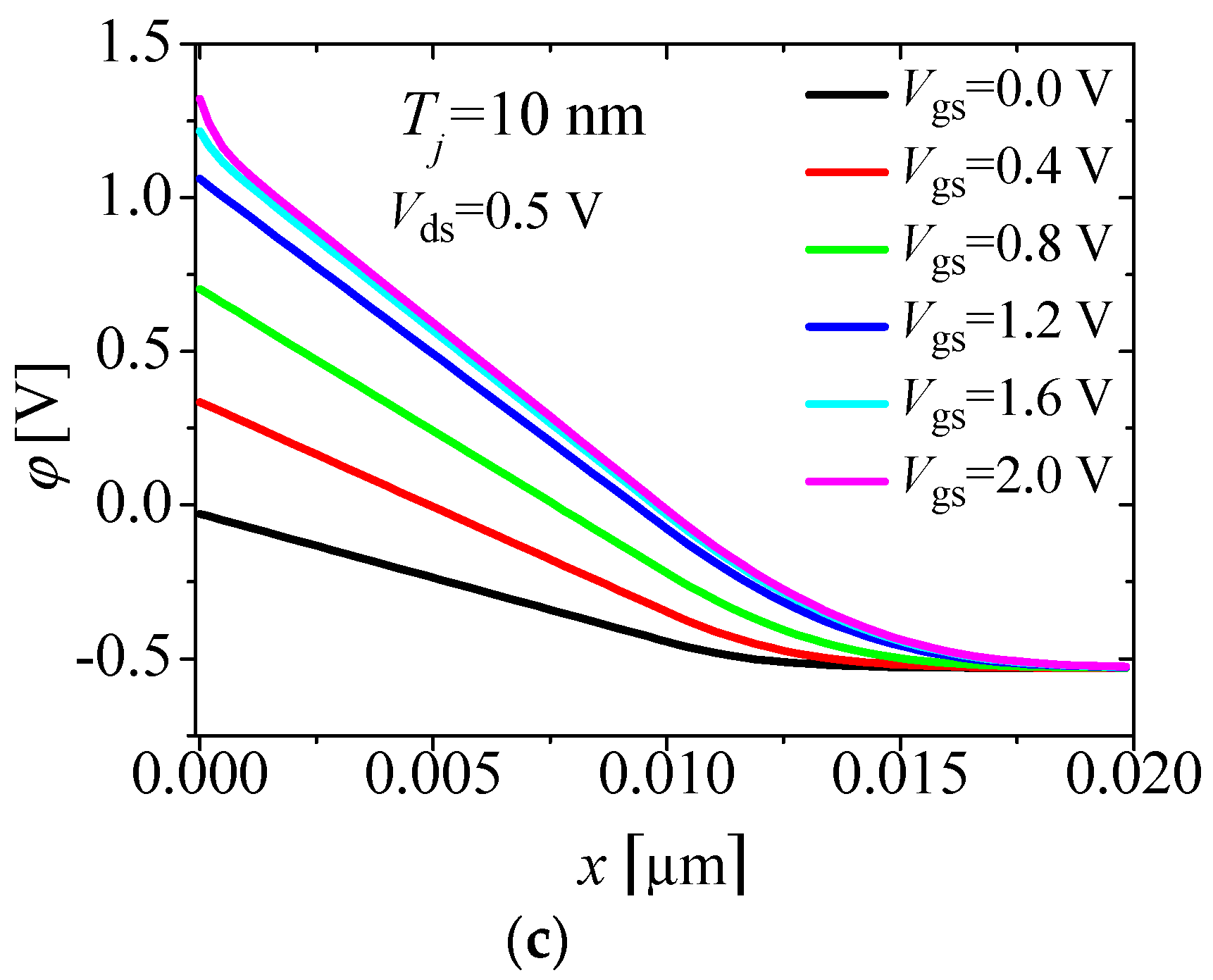
2.1. Potential Model

Figure 2a shows the TAT generation rate (GTAT) contour plot at Vgs = 0 V and Vds = 0.5 V for an LTFET with Tj = 10 nm. Figure 2b shows the GTAT extracted from the contour plot along the cutline indicated in Figure 2a, along with GTAT at several Vgs biases ranging from 0 to 2 V. The region shown along the cutline is the reference region of the model, where all parameters including potential and GTAT are calculated and assumed to be constant in the y and z directions. It can be seen that the GTAT is significant only in the channel region, and for that reason, this model calculates GTAT only in the channel region.
The potential model is based on solving the Poisson equation twice in the source and Roverlap regions. As a result, the potential and electric field (E) equations in the respective regions are given below [16]. Table 2 mentions the meaning of each symbol used in the following equations:
φ s o u r c e x s o u r c e = q N a ε s i ( x s o u r c e L d e p )
φ c h a n n e l x c h a n n e l = q N d ε s i x c h a n n e l ε o x ε s i t o x ( V g s V f b φ s )
φ s o u r c e ( x s o u r c e ) = q N a 2 ε s i ( x s o u r c e L d e p ) 2 + φ d e p
φ c h a n n e l ( x c h a n n e l ) = q N d 2 ε s i x c h a n n e l 2 ε o x ε s i t o x ( V g s V f b φ s ) x c h a n n e l + φ s
φ s = V g s V f b + q ( N a + N d ) C o x T j + q ε s i N a C o x 2 γ V g s V f b + q ( N a + N d ) 2 ε s i T j 2 + q ( N a + N d ) C o x T j + q ε s i N a 2 C o x 2 φ d e p  
where γ = 2 s i q N d / C o x . The potential profile within the channel is assumed to be linear.
φ c h a n n e l ( x c h a n n e l ) = m x c h a n n e l + φ s
where m is the slope of the linear potential profile in the channel, m = (φsφj)/Tj, or the electric field. Equation (6) is not derived from (2). It is a convenient assumption for compact modeling purposes. It can be seen in Figure 2c that potential follows a linear potential profile within the channel. Due to the strong band-bending, this assumption quasi-breaks down at higher Vgs bias. This consequence is explained later in Section 3. Because of the linear potential profile, E is constant throughout the channel and φj can be derived as
φ j = φ s + q T j 2 ( N d + 2 N a ) 2 ε s i ( 2 q N a T j 2 ) ( φ s + V b i s ) ε s i + q 2 T j 4 . ( N d N a + N a 2 ) ε s i 2

2.2. Schenk Model

The Schenk model [7,10] works by modifying the lifetime parameter (τ0) in the original Shockley–Read–Hall (SRH) recombination–generation model through the Γ parameter as follows:
τ n ( p ) = τ 0 n ( p ) 1 + Γ n ( p ) ( E )  
where n(p) in (8) represent electrons and holes, respectively. The Γ accounts for the E-driven, and phonon-assisted TAT process, and is calculated by the Schenk model. If there is any TAT present, Γ is usually significantly higher than 1 [5]. Otherwise, it is zero. The lifetime given by (8) features in the SRH model expression, which is used to give GTAT if Γ > 0, as follows:
G T A T = n p n i 2 τ 0 p 1 + Γ p ( n + n 1 ) + τ 0 n 1 + Γ n ( p + p 1 )
where ni is an intrinsic carrier concentration, n 1 = n i e x p ( E T / k T ) , p 1 = n i e x p ( E T / k T ) , and k and T are the Boltzmann constant and temperature, respectively. n and p in (9) are given by
n = n i . e x p ( φ ( x ) φ e q u a s i v t h ) ,   p = n i . e x p ( φ ( x ) v t h )  
where vth and φequasi present thermal voltage and electron quasi Fermi level, respectively. Substituting for φchannel from (6) in (10), n and p are given by
n ( x ) = n i . e x p ( m x + φ s φ q u a s i v t h ) ,   p ( x ) = n i . e x p ( m x + φ s v t h ) .
Γ is calculated by the following equation. A detailed derivation of this equation is given in [7].
Γ n ( p ) = ( 1 + ( ħ Θ n ( p ) ) 3 2 E t n ( p ) E 0 n ( p ) E 0 n ( p ) ħ ω 0 ) 1 2 ( ħ Θ n ( p ) ) 3 4 ( E t n ( p ) E 0 n ( p ) ) 1 4 2 E t n ( p ) E 0 n ( p ) ( ħ Θ n ( p ) k T ) 3 2 · e x p ( E t n ( p ) E 0 n ( p ) ħ ω 0 + ħ ω 0 k T 2 ħ ω 0 + 2 E t n ( p ) + k T 2 ħ ω 0 ln E t n ( p ) ε R E 0 n ( p ) ħ ω 0 ln E 0 n ( p ) ε R + E t n ( p ) E 0 n ( p ) k T 4 3 ( E t n ( p ) E 0 n ( p ) ħ Θ n ( p ) ) 3 2 ) .
Here, ħ is the reduced Planck’s constant, ħω0 is the effective phonon energy (Ephon), εR = SEphon is the lattice relaxation energy [17] which is known to influence the subthreshold slope (SS), where S is the Huang–Rhys factor [18] which is a measure of electron–phonon coupling. Both Ephon and S are known to influence Γ, although the effect of Ephon has been found to be dominant over S on Γ. Furthermore, the current can change if either S or Ephon change, even if εR remains constant [18]. Etn(p) is the energy at which the tunneling probability for the carriers to the tunnel from ET to the band edge is the maximum and Θ n ( p ) = (q2E2/2ħmn(p))1/3 is the electro-optical frequency [18]. mn and mp are the electron and hole tunneling masses, respectively.
The model parameters including trap level ET, S, Ephon, and n ( p ) are the fundamental quantities that strongly influence the TAT process. The first three can be determined experimentally using Deep Level Transient Spectroscopy [19,20]. The electro-optical frequency is dependent on the electric field and the tunneling masses. This restricts the model to being a local TAT model [18]. E0n(p) is the energy of an optimum horizontal transition path which is dependent on the field strength and temperature. This determines the most probable recombination path [18], and is given by
E 0 n ( p ) = 2 ε F n ( p ) [ ε F n ( p ) + E t n ( p ) + ε R ε F n ( p ) ] ε R
where ε F n ( p ) = ( 2 ε F k T ) 2 ( ħ Θ n ( p ) ) 3 . Etn for electrons is given by
E t n = 1 2 E b g n + 3 4 k T ln ( m n m p ) E T ( 32 R c ħ 3 Θ 3 ) 1 4
and Etp is given by
E t p = 1 2 E b g n + 3 4 k T ln ( m n m p ) E T + ( 32 R v ħ 3 Θ 3 ) 1 4
where Rc(v) are the effective Rydberg energies; Rc(v) = mn(p)Ry2 for electrons (holes), where Ry (= 13.6 eV) is the Rydberg energy and ε is the permittivity.

2.3. Compact Implementation
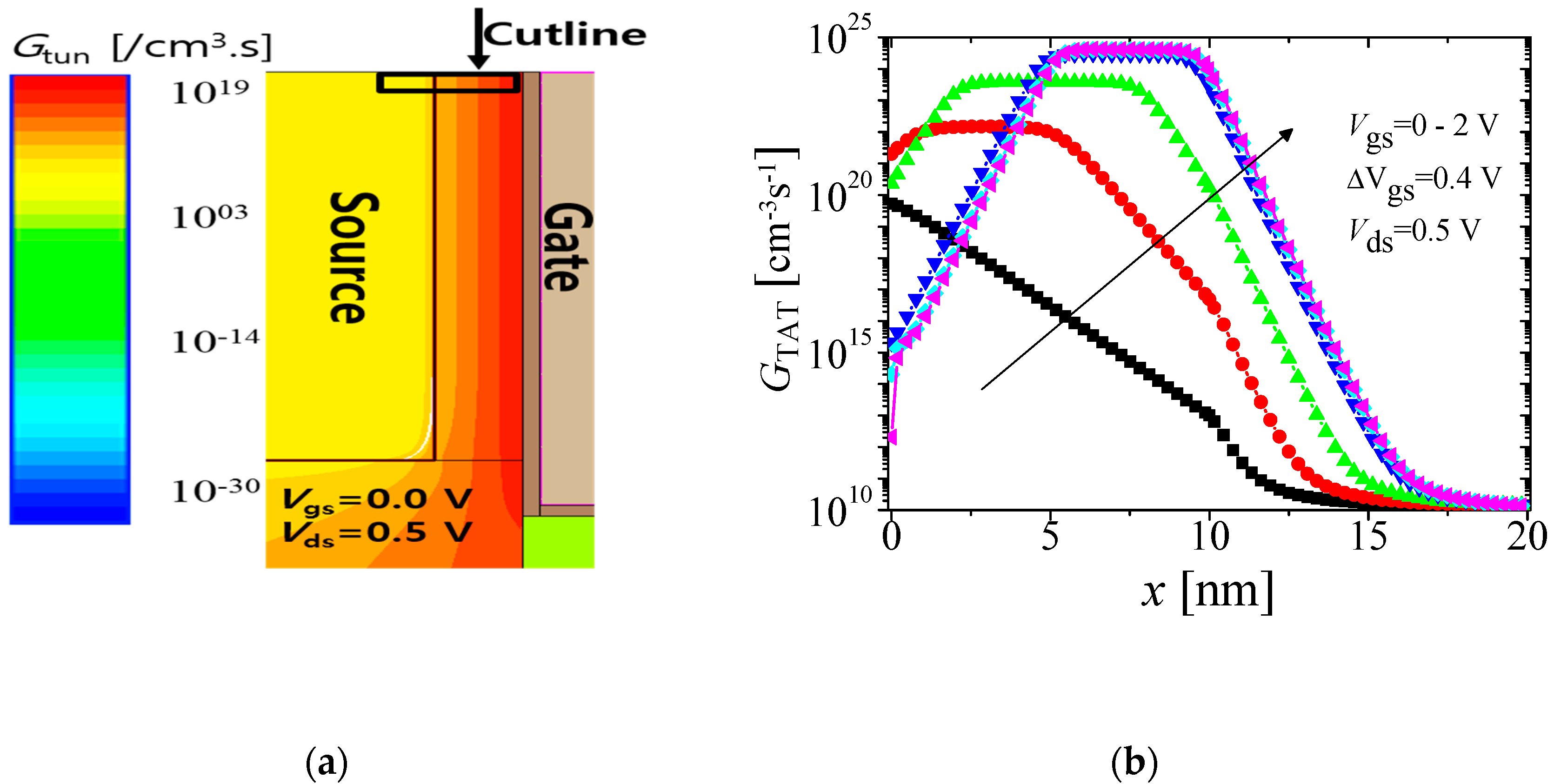
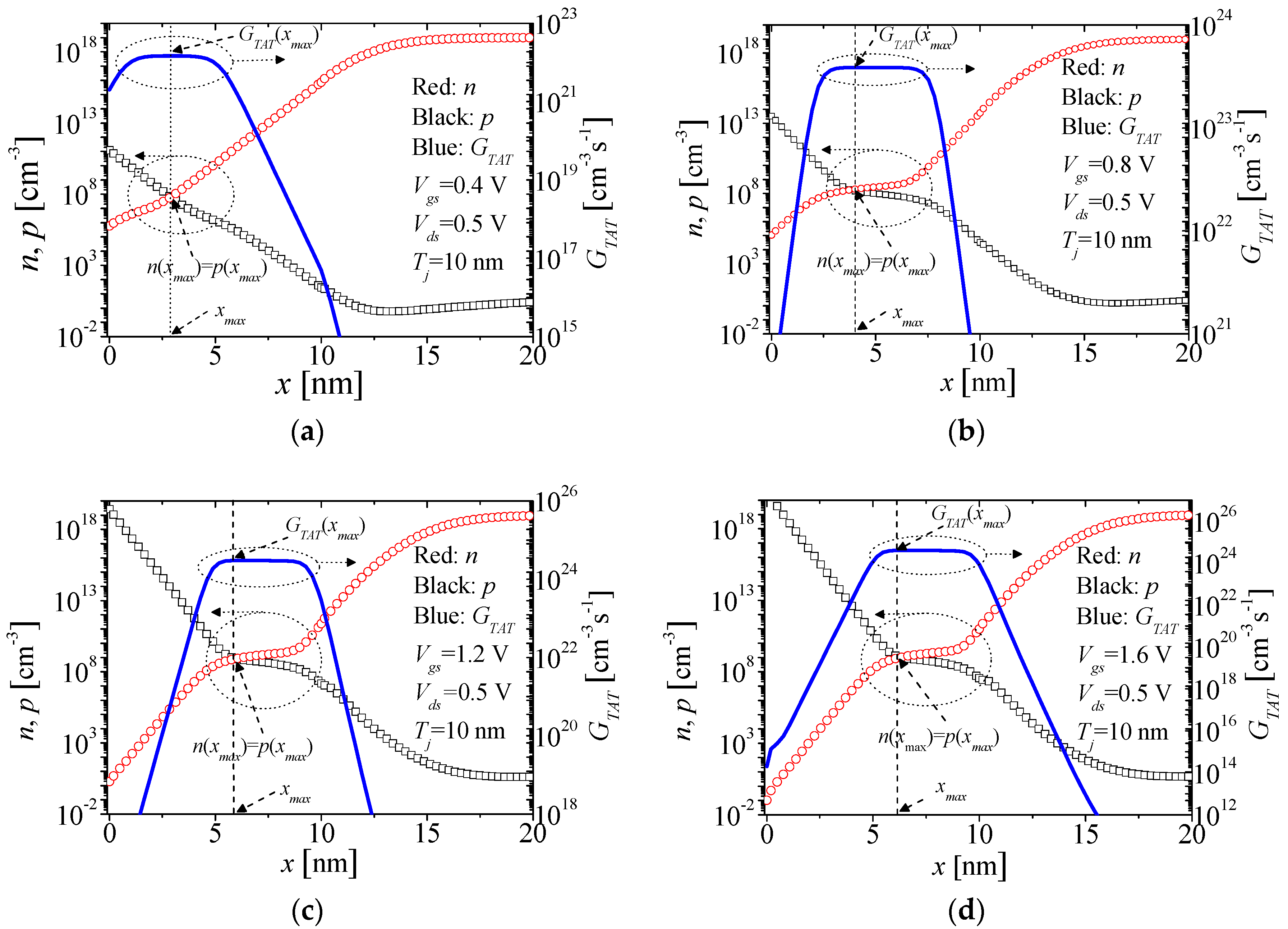
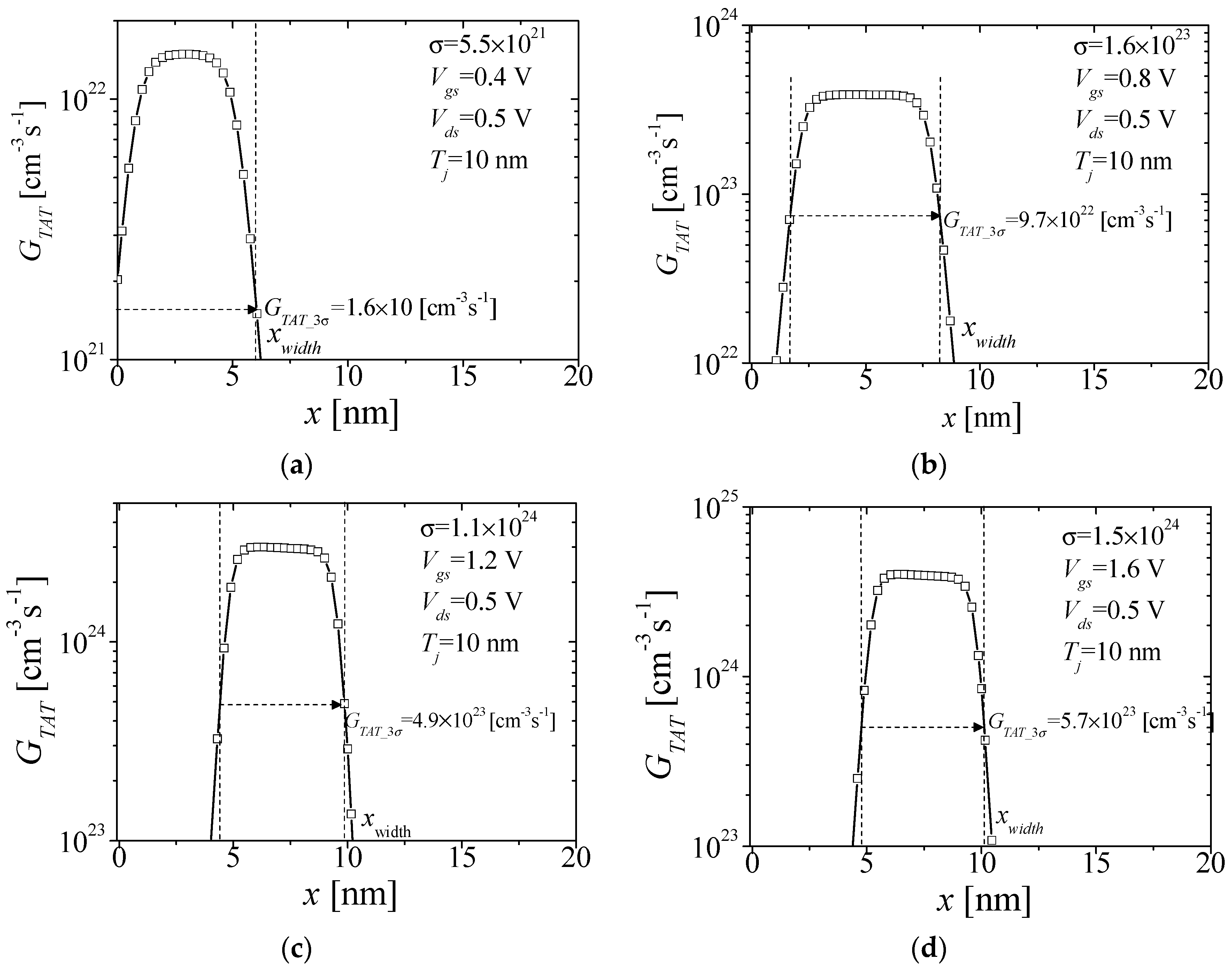
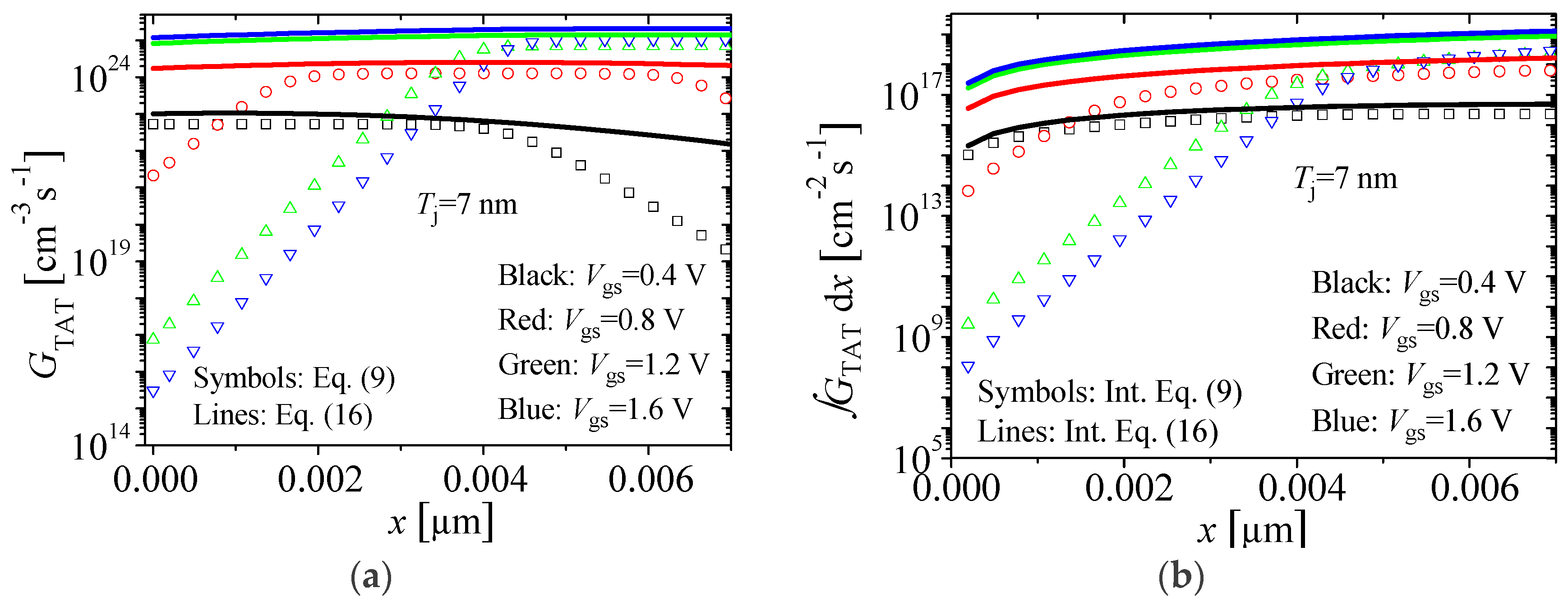
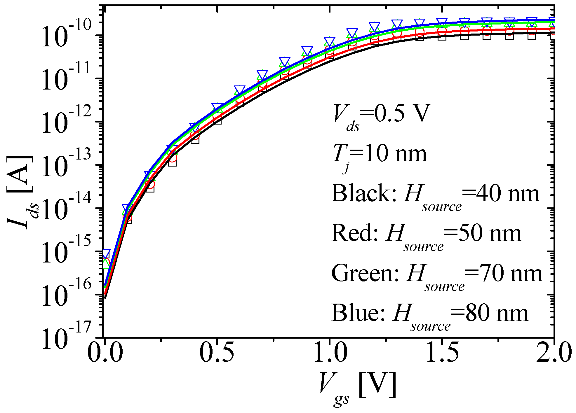
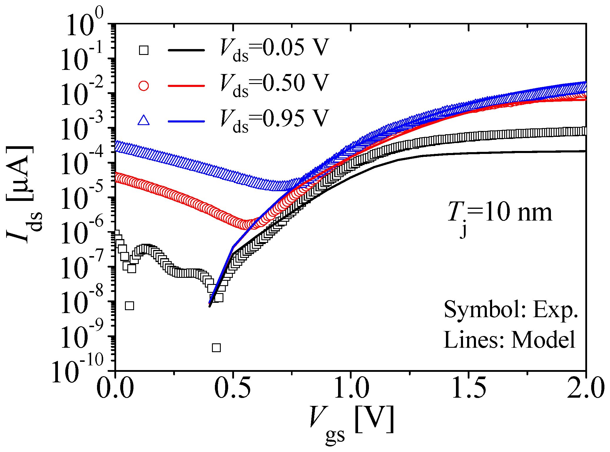
For compact implementation, GTAT given by (9) is approximated using a Gaussian distribution function as follows:
G T A T = G T A T _ m a x e x p ( ( x x m a x x w i d t h   ) 2 )
where xwidth is the width of the Gaussian distribution. GTAT_max is the maximum GTAT along the channel region, and xmax is the x-point where GTAT is maximum. GTAT_max always occurs where n = p. This can be seen in Figure 3 which shows n, p (left axis), and GTAT (right axis) at different Vgss for Vds=0.5 V, for an LTFET with Tj = 10 nm. It can be seen from Figure 3 that at the point where n = p, GTAT is maximum. The x co-ordinate where this occurs is labelled as xmax. xmax can be found by equating n = p, as follows: and solving for x, that is.
n i e x p ( m x m a x + φ s φ e q u a s i v t h ) = n i e x p ( m x m a x + φ s v t h )
x m a x = φ e q u a s i ( 2 φ s ) 2 m
GTAT_max is found by using xmax in (9), as follows:
G T A T _ m a x = n ( x m a x ) p ( x m a x ) n i 2 τ 0 p 1 + Γ p [ n ( x m a x ) + n 1 ] + τ 0 n 1 + Γ n [ p ( x m a x ) + p 1 ]
where n(xmax) and p(xmax) can be found using x = xmax in (11). It should be mentioned that Γ is independent of x; constant electric field in the channel makes Γ calculated from (12) essentially independent of x. In order to find xwidth, the standard deviation (σ) of the Gaussian distribution is utilized. σ is obtained using standard equations [21]. Utilizing the Empirical Rule in Statistics and Probability [21] which states that 99.7% of values in a normal distribution lie within 3 standard deviations of the mean value [21], the width of Gaussian distribution was approximated at 3 standard deviations of the maximum value of the function, that is, the width was estimated to be the x co-ordinate (xwidth) that satisfied this condition, 3 σ   o f   G T A T , symbolized by G T A T _ 3 σ . Substituting this condition in (9), along with (11), assuming mid-gap trap level so that n1 = p1 = ni, (9) can be given by
G T A T _ 3 σ   = n i 2 e x p ( φ q u a s i v t h ) n i 2 τ 0 p 1 + Γ p ( n + n i ) + τ 0 n 1 + Γ n ( p + n i )
It can be seen from Figure 3 and Figure 4 that at any bias, the width of the Gaussian distribution n >> p. Furthermore, assuming equivalent τ0n = τ0p = τ0, and Γn~Γp which is true for the materials with me~mp including silicon, and advanced III-V InGaAs-based materials [13], (20) can be expressed as
G T A T _ 3 σ   = n i 2 e x p ( φ q u a s i v t h ) n i 2 τ 0 1 + Γ n [ n i ( e x p   ( m x w i d t h + φ s φ q u a s i v t h ) + 2 ) ]
Taking log on both sides, ignoring 2, and solving for xwidth, xwidth can be given by
x w i d t h = { log [ ( G T A T _ 3 σ   ) ( τ 0 1 + Γ n ) ] log ( n i ) } . ( v t h φ s ) m
The TAT drain current (Ids_TAT) is given by the following expression:
I d s _ T A T = q 0 a b s ( T j ) 0 H s o u r c e 0 W G T A T d x d y d z = q W H s o u r c e 0 a b s ( T j ) G T A T d x
I d s _ T A T = π q W H s o u r c e G T A T _ M a x x w i d t h [ e r f ( a b s ( T j ) x max x w i d t h ) e r f ( 0 x m a x x w i d t h ) ]
where W is the width of the device. It is assumed that GTAT is independent of Hsource, and W. Note that (24) is simply the closed-integral expression of (16) integrated between Tj and 0 μm at the surface.

3. Results

To demonstrate whether the Gaussian approximation of GTAT is feasible, Figure 5 compares GTAT calculated from the actual SRH-based GTAT equation: (9) and GTAT approximated by Gaussian approximation: (16) for Tj = 7 nm. The approximated GTAT is reasonably consistent with the calculated GTAT. It should be emphasized that this is only an approximation for compact modeling purposes. The approximated GTAT overestimates the actual GTAT, particularly at high bias values. The overestimation at higher Vgs bias is because the linear potential profile assumption does not remain valid at high Vgs bias. Figure 5b shows two integrated GTAT. Based on Figure 5a,b, some overestimation of Ids_TAT can be expected at high Vgs bias.
Figure 6 compares Ids_TAT from the technology computer-aided design (TCAD) (symbol) against Ids_TAT calculated from (24) for different Tj. Considering that this is a compact model, a reasonable agreement on the simulation results between the TCAD and the model is observed. The expected overestimation in Ids_TAT at high Vgs bias can be seen in Figure 6. Figure 7 compares Ids_TAT from the TCAD (symbols) against Ids_TAT calculated from the model for Tj = 10 nm and different Hsource, at Vds = 0.5 V. The slight disagreement at higher bias is due to the linear potential approximation which is not very accurate at higher bias due to strong surface band bending.
To truly test the relevancy of the model, the model was used to fit experimental data from [12]. It was found in [13] that Ids_TAT dominates the entire Vgs range for all Vds biases. Therefore, Ids_TAT from the model was compared against the experimental data. The result is shown in Figure 8. The model was calibrated to match the experimental IdsVgs characteristics at Vds = 0.95 V by choosing τ0 = 10−11 s. The model follows the experimental Ids trend very well. However, it is not entirely accurate, especially at low Vds. The reason for this is that (1) the electrostatic degradation caused by the trap states was not considered in this work. Electrostatic degradation causes the potential to degrade, and this effect becomes more important at high bias. To account for that, the Poisson and trap charge need to be calculated self-consistently. Furthermore, a different potential profile expression other than the linear potential profile given by (6) will be needed. This is because with the traps causing electrostatic degradation, the degraded potential profile changes from being linear to non-linear. It should be emphasized that from Figure 1b, BTBT current calculated using experimentally determined Ak/Bk parameters was found to be too low than the current of the experimental device. The absence of BTBT current in this particular example is not the result of mismatch. An ambipolar current was also found to be a factor in the experimental device which could be important at low Vgs bias. The other reasons possibly include the use of abrupt doping profiles, and abrupt geometry in the simulation. The limitations of the model include the use of one trap at the mid-gap level, and the lack of electrostatic degradation.

4. Conclusions

The literature lacks a compact tunable trap-assisted-tunneling model. This work presented a compact TAT model that captured important physical parameters that influence the TAT process including phonon energy, the Huang–Rhys factor, and tunneling masses. The model is divided into three parts. The first part includes the potential model, the second part includes the standard Schenk model equations, and the third part includes the compact implementation of the Schenk model where the TAT tunneling rate is expressed as a Gaussian distribution. The approximated Gaussian distribution is then integrated along the x-axis to generate a TAT-generated drain current. The model was tested against the TCAD data and was found to be in reasonable agreement. The model was also tested against Ids from an experimental device. The model was found to follow the same trend as the experimental device. The result, however, was not truly accurate. This could be due to neglecting the electrostatic degradation caused by the traps which could be important at high bias. Another reason for the inaccuracy could be neglecting effects such as contact resistance in the model. In summary, this work provides a useful contribution within the compact trap-assisted-tunneling modeling domain of TFET devices. The compact implementation part of the model can be generalized for use in any TFET device and can easily be incorporated in the simulation program with integrated circuit emphasis (SPICE) framework. For the completed compact model of the TET for SPICE implementation, series resistance [22], SRH [23], ambipolar, quantum confinement [24], and breakdown models [25] should be added to this proposed model.

Author Contributions

Conceptualization, Y.S.Y. and F.N.; Data curation, Y.S.Y. and F.N.; Formal analysis, Y.S.Y. and F.N.; Investigation, F.N.; Methodology, F.N.; Project administration, Y.S.Y.; Supervision, Y.S.Y.; Visualization, F.N.; Writing—original draft, F.N.; Writing—review and editing, Y.S.Y. All authors have read and agreed to the published version of the manuscript.

Funding

This research was funded by the Ministry of Trade, Industry, and Energy (MOTIE), project number 10054888 and Korea Semiconductor Research Consortium (KSRC) support program for the development of future semiconductor devices.

Acknowledgments

This work was supported by IDEC (EDA tool).

Conflicts of Interest

The authors declare no conflict of interest.

References

  1. Boucart, K.; Ionescu, A. Double-gate tunnel FET with high-κ gate dielectric. IEEE Trans. Electron. Devices 2007, 54, 1725–1733. [Google Scholar] [CrossRef]
  2. Flori, G.; Iannaccone, G. Ultra-voltage bilayer graphene tunnel FET. IEEE Electron. Device Lett. 2009, 30, 1096–1098. [Google Scholar]
  3. Datta, S.; Liu, H.; Narayan, V. Tunnel FET Technology: A Reliability Perspective. Microelectron. Reliab. 2014, 54, 861–874. [Google Scholar] [CrossRef]
  4. Alian, A.; Mols, Y.; Bordallo, C.C.M.; Verreck, D.; Verhulst, A.; Vandooren, A.; Rooyackers, R.; Agopian, P.G.D.; Martino, J.A.; Thean, A.; et al. InGaAs tunnel FET with sub-nanometer EOT and sub-60 mV/dec sub-threshold swing at room temperature. Appl. Phys. Lett. 2016, 109, 243502. [Google Scholar] [CrossRef] [Green Version]
  5. Sajjad, R.N.; Chern, W.; Hoyt, J.L.; Antoniadis, D.A. Trap assisted tunneling and its effect on subthreshold swing of tunnel FETs. IEEE Trans. Electron. Devices 2016, 63, 4380–4387. [Google Scholar] [CrossRef]
  6. Sajjad, R.N.; Antoniadis, D. A compact model for tunnel FET for all operating regimes including trap assisted tunneling. In Proceedings of the 2016 74th Annual Device Research Conference (DRC), Newark, DE, USA, 19–22 June 2016. [Google Scholar]
  7. Hurkx, G.A.M.; Klassen, D.B.M.; Knuvers, M.P.G. A new recombination model for device simulation including tunneling. IEEE Trans. Electron. Devices 1992, 39, 331–338. [Google Scholar] [CrossRef]
  8. Jiménez-Molinos, F.; Palma, A.; Gámiz, F.; Banqueri, J.; López-Villanueva, J.A. Physical model for trap-assisted inelastic tunneling in metal-oxide-semiconductor structures. J. Appl. Phys. 2001, 90, 3396–3404. [Google Scholar] [CrossRef]
  9. Schenk, A.; Sant, S.; Moselund, K.; Riel, H. The impact of hetero-junction and oxide-interface traps on the performance of InAs/Si tunnel FETs. In Proceedings of the 2017 17th International Workshop on Junction Technology, Uji, Japan, 1–2 June 2017. [Google Scholar]
  10. Synopsys. User Manual, Version L-2016.03, Synopsys TCAD Sentaurus; Synopsys: San Jose, CA, USA, 2016. [Google Scholar]
  11. Schenk, A. A model for the field and temperature dependence of Shockley–Read–Hall lifetimes in silicon. Solid-State Electron. 1992, 35, 1585–1596. [Google Scholar] [CrossRef]
  12. Kim, S.W.; Kim, J.H.; Liu, T.K.; Choi, W.Y.; Park, B. Demonstration of L-shaped tunnel field-effect transistors. IEEE Trans. Electron. Devices 2016, 63, 1774–1778. [Google Scholar] [CrossRef]
  13. Najam, F.; Yu, Y.S. Physically consistent method for calculating trap-assisted-tunneling current applied to line tunneling field-effect-transistor. IEEE Trans Electron. Devices 2020, 67, 2106–2112. [Google Scholar] [CrossRef]
  14. Vandenberghe, W.G.; Verhulst, A.S.; Groeseneken, G.; Soree, B.; Magnus, W. Analytical model for point and line tunneling in a tunnel field-effect transistor. In Proceedings of the 2008 International Conference on Simulation of Semiconductors Processes and Devices, Hakone, Japan, 9–11 September 2008. [Google Scholar]
  15. Najam, F.; Yu, Y.S. Investigation of corner effect and identification of tunneling regimes in L-shaped tunnel field-effect-transistor. J. Nanosci. Nanotechnol. 2018, 18, 6578–6583. [Google Scholar] [CrossRef] [PubMed]
  16. Najam, F.; Yu, Y.S. Compact model for L-shaped tunnel field-effect transistor including the 2D region. Appl. Sci. 2019, 9, 3716. [Google Scholar] [CrossRef] [Green Version]
  17. Smets, Q.; Verhulst, A.S.; Simeon, E.; Gundlach, D.; Richter, D.; Collaert, N.; Heyns, M.M. Calibration of bulk trap-assisted tunneling and Shockley–Read–Hall currents and impact on InGaAs tunnel-FETs. IEEE Trans. Electron. Devices 2017, 64, 3622–3626. [Google Scholar] [CrossRef]
  18. Mandurrino, M.; Goano, M.; Vallone, M.; Bertazzi, F.; Ghione, G.; Verzellesi, G.; Meneghini, M.; Meneghesso, G.; Zanoni, E. Semiclassical simulation of trap-assisted tunneling in GaN-based light-emitting diodes. J. Comput. Electron. 2015, 14, 444–445. [Google Scholar] [CrossRef]
  19. Vincent, G.; Chantre, A.; Bois, D. Electric field effect on the thermal emission of traps in semiconductor junctions. J. Appl. Phys. 1972, 50, 5484–5487. [Google Scholar] [CrossRef]
  20. Fleming, R.M.; Seager, C.H.; Lang, D.V.; Campbell, J.M. Injection deep level transient spectroscopy: An improved method for measuring capture rates of hot carriers in semiconductors. J. Appl. Phys 2015, 118, 015703. [Google Scholar] [CrossRef]
  21. Mendenhall, W.; Beaver, R.J.; Beaver, B.M. Introduction to Probability and Statistics Metric Edition, 15th ed.; Cengage Learning US: Boston, MA, USA, 2019. [Google Scholar]
  22. Klassen, F.; Biermans, P.; Velghe, R. The series resistance of submicron MOSFETs and its effect on their characteristics. J. Phys. Colloq. 1988, 49, C4-257–C4-260. [Google Scholar] [CrossRef]
  23. Liu, Y.; Yan, J.; Wang, H.; Han, G. Temperature dependent IDSVGS characteristics of an N-channel Si tunneling field-effect transistor with a germanium source on Si(110) substrate. J. Semicond. 2014, 35, 024001. [Google Scholar] [CrossRef]
  24. Walke, A.M.; Verhulst, A.S.; Vandooren, A.; Verreck, D.; Simoen, E.; Rao, V.R.; Groeseneken, G.; Collaert, N.; Thean, A.V.Y. Part I: Impact of field-induced quantum confinement on the subthreshold swing behavior of line TFETs. IEEE Trans. Electron. Devices 2013, 60, 4057–4064. [Google Scholar] [CrossRef]
  25. Jung, H.; Dimitrijev, S. Analysis of flat-band-voltage dependent breakdown voltage for 10 nm double gate. MOSFET. J. Inf. Commun. Converg. Eng. 2018, 16, 43–47. [Google Scholar]
Figure 1. (a). Schematic of the L-shaped tunneling field-effect-transistor (LTFET). (b) Black: IdsVgs characteristics of experimental LTFET [12], blue: trap-assisted-tunneling (TAT) current calculated using the trap distribution and method in [13], and red: Band-to-band tunneling (BTBT) current fitted using dynamic nonlocal BTBT current [10].
Applsci 10 04475 g001
Figure 2. (a) GTAT contour plot at Vgs = 0 and Vds = 0.5 V for an LTFET with Tj = 10 nm. (b) GTAT extracted along the cutline in Figure 2a, for Vgs = 0–2 V with ΔVgs = 0.4 V. (c) Potential along the cutline of Figure 2a at different Vgss for Vds = 0.5 V and Tj = 10 nm.
Applsci 10 04475 g002aApplsci 10 04475 g002b
Figure 3. (ad) n, p (left-axis), and GTAT (right-axis) at Vgs = 0.4, 0.8, 1.2, and 1.6 V, respectively, all at Vds = 0.5 V. The location where n = p, and of GTAT_Max, that is at x = xmax are identified by arrows.
Applsci 10 04475 g003
Figure 4. (ad) Illustration of the method used to estimate the width of the Gaussian distribution. GTAT is shown, and xwidth is pointed out by arrows, for Vgs = 0.4, 0.8, 1.2, and 1.6 V, respectively.
Applsci 10 04475 g004
Figure 5. (a) GTAT calculated from Equation (9) (symbols) compared against GTAT calculated from Equation (16) (lines) for Vgs = 0.4, 0.8, 1.6, and 2.0 V shown by black, red, green and blue colors respectively, for Vds = 0.5 V and Tj = 7 nm. (b) Integrated GTAT, T j 0 G T A T d x shown in Figure 5a. Same annotation as Figure 5a except symbols: Integral of Equation (9), and lines: Integral of Equation (16).
Applsci 10 04475 g005
Figure 6. Ids_TAT from technology computer-aided design (TCAD) (symbols) compared with Ids_TAT calculated from (24) for Tj = 7 nm (a), 8 nm (b), 9 nm (c) and 10 nm (d). Black, blue, and red represent Vds = 0.25, 0.5, and 0.95 V, respectively.
Applsci 10 04475 g006
Figure 7. Ids from TCAD (symbols) versus Ids calculated by the model for an LTFET with Tj = 10 nm, and different Hsource = 40 nm (black), 50 nm (red), 70 nm (green) and 80 nm (blue) at Vds = 0.5 V.
Applsci 10 04475 g007
Figure 8. Ids from the experimental device (symbols) [12] compared with Ids_TAT calculated from (23).
Applsci 10 04475 g008
Table 1. Current mechanisms in line tunneling TFETs and their threshold voltages.
MechanismRegion DominatedThreshold Voltage
2D BTBTTypically intermediate bias region.TAT < 2D BTBT < 1D BTBT
1D BTBTTypically subthreshold region.
TATTypically subthreshold and intermediate bias regions [5], and in extreme cases [13] the high bias region as well.
Table 2. List of symbols specifically used in (1)–(7).
SymbolDescriptionValue/Unit
φsourcePotential at source edgeV
Na, NdSource, channel doping cm−3
xsource, xchannelx co-ordinate in source, channelcm
LdepDepletion length in sourcecm
εsi, εoxSilicon, oxide permittivity11.9Ɛ0, 25Ɛ0
Vfb,Flat band voltageV
qElectron charge1.6 × 10−19 C
φs,φj,φchannelSurface potential at xchannel = 0, junction potential at x = Tj, and potential as a function of xchannel, respectivelyV
φ;depDepletion potential in sourceV
CoxGate capacitanceF/cm2
VbisChannel/source junction built-in potentialV

